Transmissive diffraction grating, and spectral separation element and spectroscope using the same
a spectral separation element and grating technology, applied in the direction of optical radiation measurement, instruments, spectrometry/spectrophotometry/monochromators, etc., can solve the problems of difficult to keep the width of the ridge constant, difficult to manufacture, and difficult to keep the width constant. , to achieve the effect of suppressing the deterioration of characteristics and easy fabrication
- Summary
- Abstract
- Description
- Claims
- Application Information
AI Technical Summary
Benefits of technology
Problems solved by technology
Method used
Image
Examples
embodiment 1
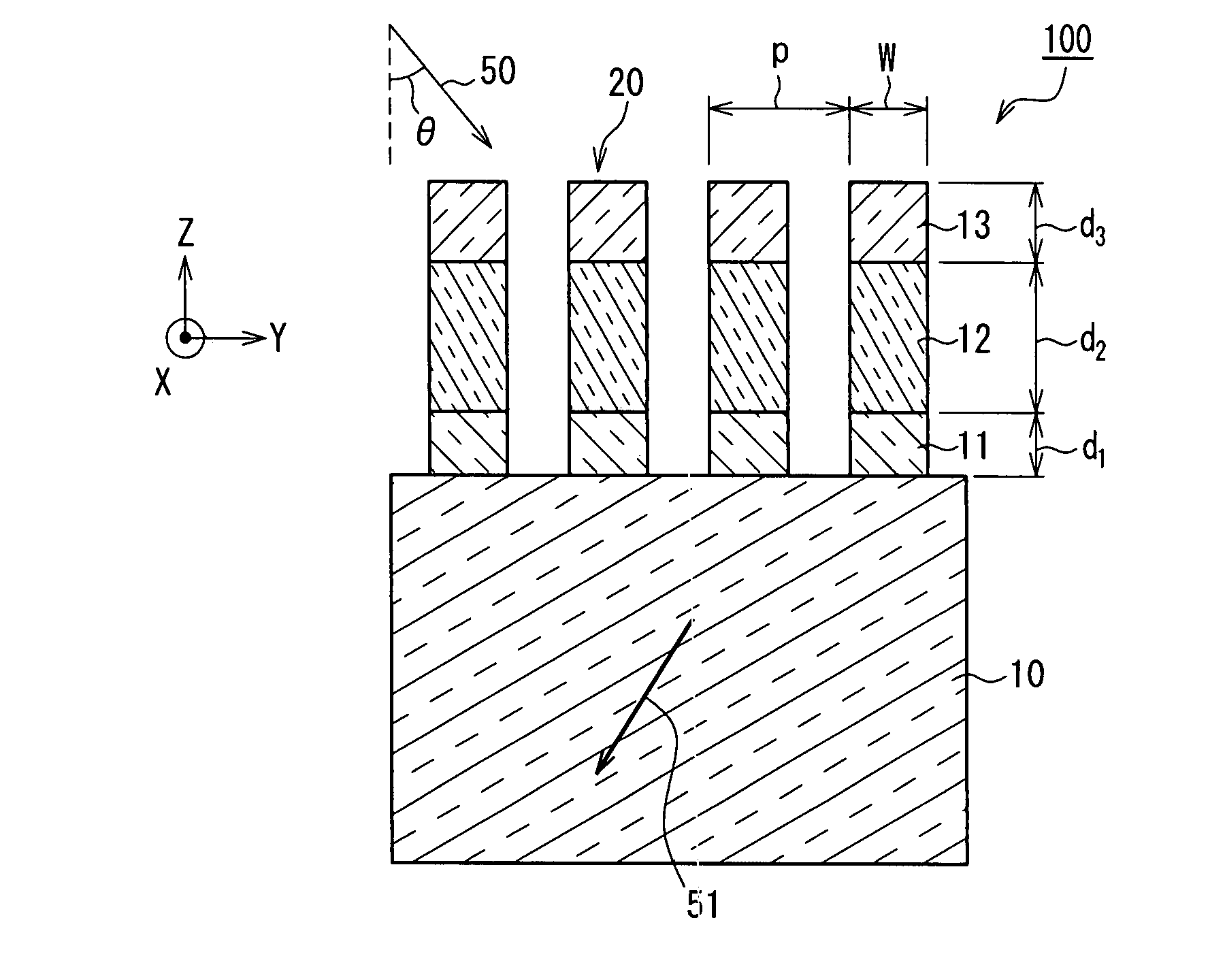
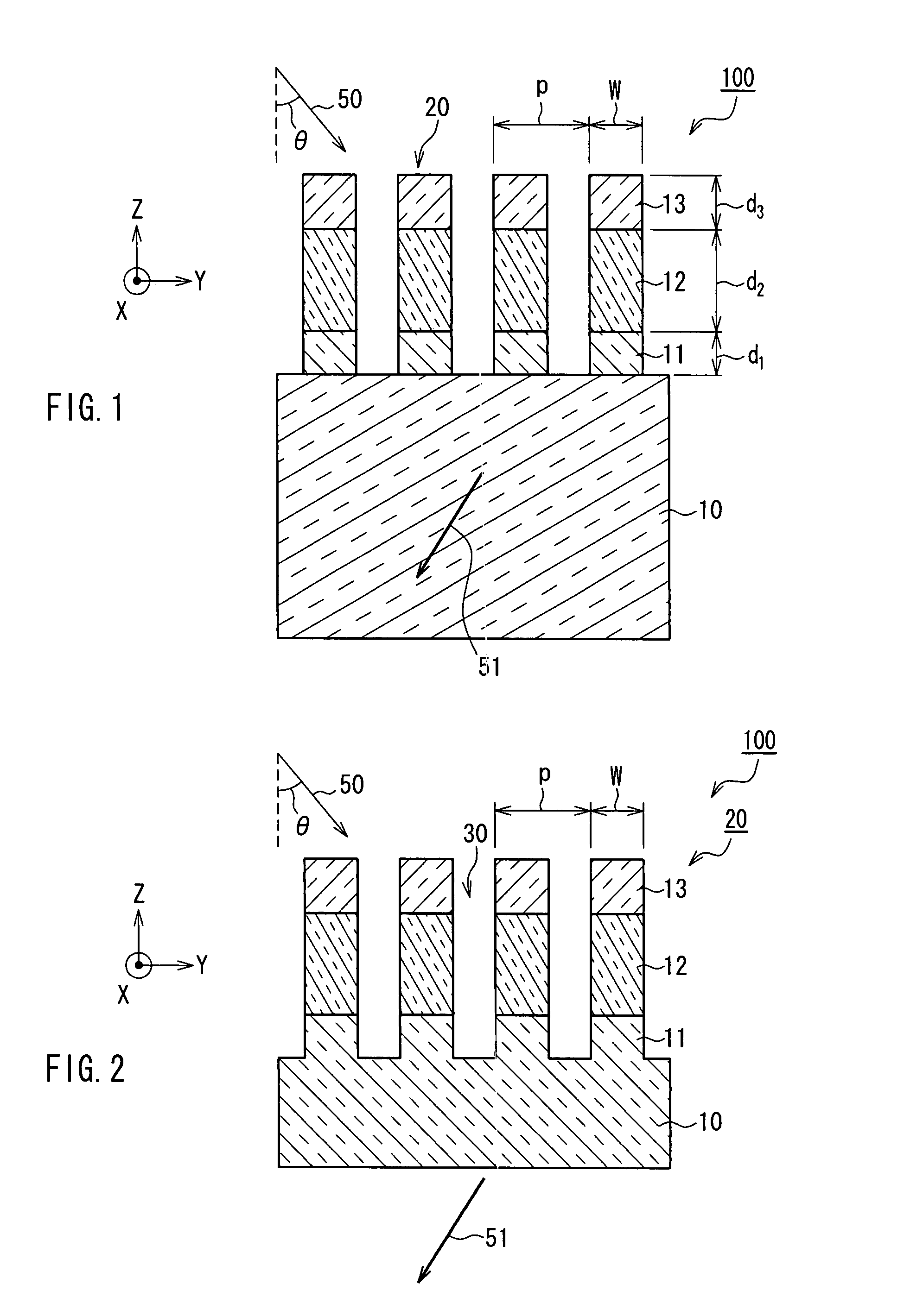
[0071]FIG. 1 is a cross-sectional view schematically illustrating a transmissive diffraction grating in Embodiment 1 of the present invention.
[0072]As shown in FIG. 1, a transmissive diffraction grating (which is referred simply to as “diffraction grating” below) 100 of the present embodiment includes a substrate 10 and a plurality of rectangular ridges 20 provided in a mutually parallel manner at constant periodicity p on the substrate 10. Here, the ridges 20 are made of three layers arranged in succession from the substrate 10 outward: a first low refractive index layer (first layer) 11, a high refractive index layer (second layer) 12, and a second low refractive index layer (third layer) 13. The high refractive index layer 12 has a higher refractive index in comparison with the first low refractive index layer 11 and second low refractive index layer 13. In the present specification, the term “high refractive index layer” is used to refer to a layer made of material with a refrac...
example 1
DESIGN EXAMPLE 1
[0100]First of all, explanations are provided regarding Design Example 1.
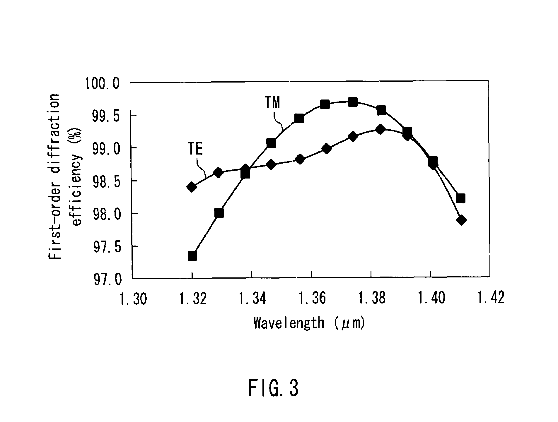
[0101]Results obtained in Design Example 1 are listed below (Table 1). In Design Example 1, the angle of incidence 0 onto the diffraction grating face was set to 45°, the periodicity p of the diffraction grating to 1 μm, the refractive index n2 of the high refractive index layer 12 to 2.10, and the refractive index n1 of the first low refractive index layer 11, the refractive index n3 of the second low refractive index layer 13, and the refractive index ns of the substrate 10 to 1.46, while the other parameters were optimized, including the thickness d1 of the first low refractive index layer 11, the thickness d2 of the high refractive index layer 12, the thickness d3 of the second low refractive index layer 13, and the width W of the ridges 20. The optimization was carried out with a view to increase the maximum value of diffraction efficiency as much as possible.
[0102]
TABLE 1RefractiveRefracti...
example 2 to 5
DESIGN EXAMPLE 2 to 5
[0116]Design examples 2 to 5 will be explained next.
[0117]The diffraction efficiency results of Design Examples 2 to 5 are shown in FIGS. 9 to 12, with the preset values being as indicated above (Table 1). In Design Examples 2 to 5, the angle of incidence θ onto the diffraction grating face was set to 50°, the periodicity p of the diffraction grating to 1 μm, the refractive index n1 of the first low refractive index layer 11, the refractive index n3 of the second low refractive index layer 13, and the refractive index n, the substrate 10 to 1.46, while the other parameters were optimized, including the thickness d1 of the first low refractive index layer 11, the thickness d2 of the high refractive index layer 12, the thickness d3 of the second low refractive index layer 13, and the width W of the ridges 20. Moreover, in Design Examples 2 to 4, the refraction indices n2 of the high refractive index layer 12 were set, respectively, to 2.18, 2.14, and 2.10 and each...
PUM
 Abstract
Description
Claims
Application Information


