Wireless IC tag and process for manufacturing the same

a technology of ic tags and wires, applied in the direction of instruments, resonant antennas, burglar alarm mechanical actuation, etc., can solve the problems of loss of cost efficiency, increase in physical size, radio wave interference by antennas, etc., and achieve simple and effective wireless ic tags, excellent economic efficiency, and compact size

Inactive Publication Date: 2010-04-06
HITACHI LTD
View PDF15 Cites 2 Cited by
  • Summary
  • Abstract
  • Description
  • Claims
  • Application Information

AI Technical Summary

Benefits of technology

[0012]An object of the present invention is to provide a wireless IC tag that has strength in congestion control tolerant of the influence of radio wave interference in a state in which plural wireless IC tags exist within electromagnetic waves from a reader and are multi-read.
[0013]Another object of the present invention is to provide a wireless IC tag which is compact in size, has high productivity, and excellent economic efficiency, and which has strength in congestion control tolerant of the influence of radio wave interference.
[0014]Another object of the present invention is to provide a wireless IC tag that has various usage patterns and reading forms and has strength in congestion control tolerant of the influence of radio wave interference in any states.
[0021]According to the present invention, a wireless IC tag can be formed which is compact in size, has excellent economic efficiency, and is tolerant of radio wave interference, which has been impossible with conventional wireless IC tags. By narrowing down the size of an antenna, in comparison with a wide antenna, a simple and effective wireless IC tag has been formed with reduction in the shade and a reflection amount of radio waves which will cause radio wave interference.

Problems solved by technology

Since a wireless IC tag has antenna conductors, a problem of radio wave interference by the antenna occurs in wireless IC tags having a congestion control function.
In such a system, problems such as an increase in physical size due to the relay elements and the loss of cost efficiency exist, and the formation of small-sized wireless IC tags and economical wireless IC tags is difficult.
However, no reference is made to the problem of radio wave interference when plural wireless tags are in an area of electromagnetic waves.
The technology does not solve the problem of radio wave interference.
Rather, the technology amplifies this problem because of the lack of constraints on antenna size.
In a state in which plural wireless IC tags exist within electromagnetic waves from a reader and are multi-read, as disclosed in Japanese Patent Laid-Open No. 2000-332523, wireless IC tags with a wide antenna width are problematic in that they are susceptible to the influence of radio wave interference because of the existence of the shade of radio waves.

Method used


Image

  • Wireless IC tag and process for manufacturing the same
  • Wireless IC tag and process for manufacturing the same
  • Wireless IC tag and process for manufacturing the same

Examples


first embodiment

[0050]A first embodiment of the present invention will be described with reference to FIGS. 1 to 13.

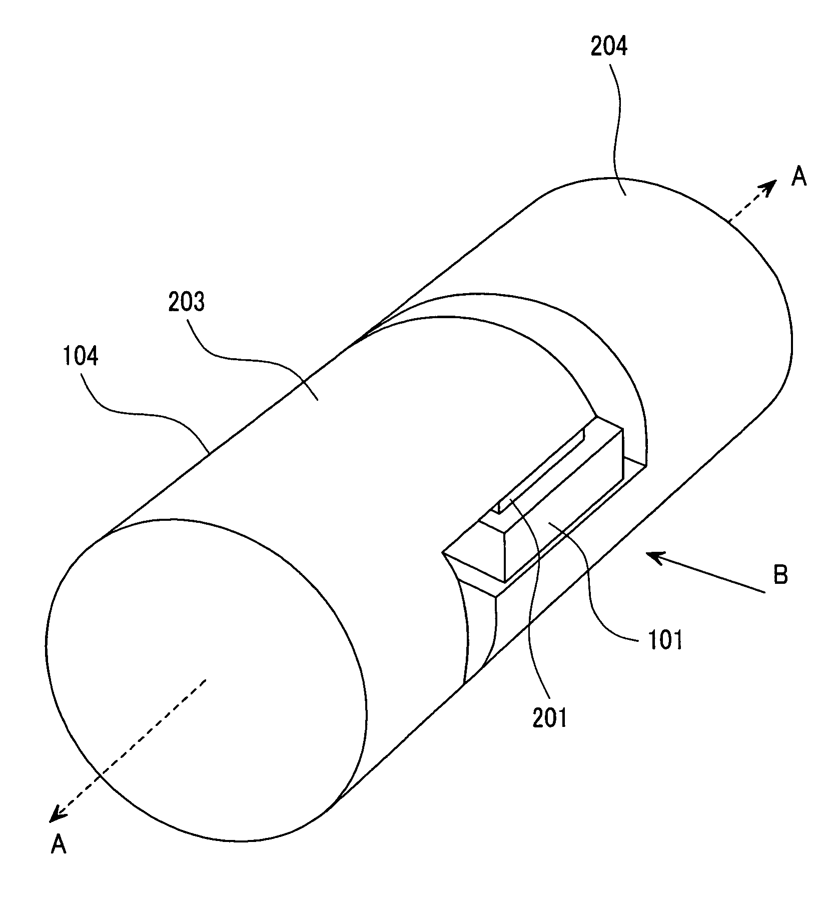
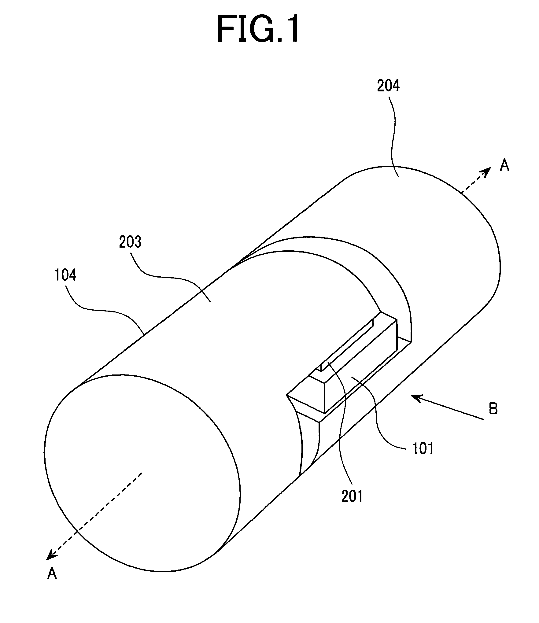
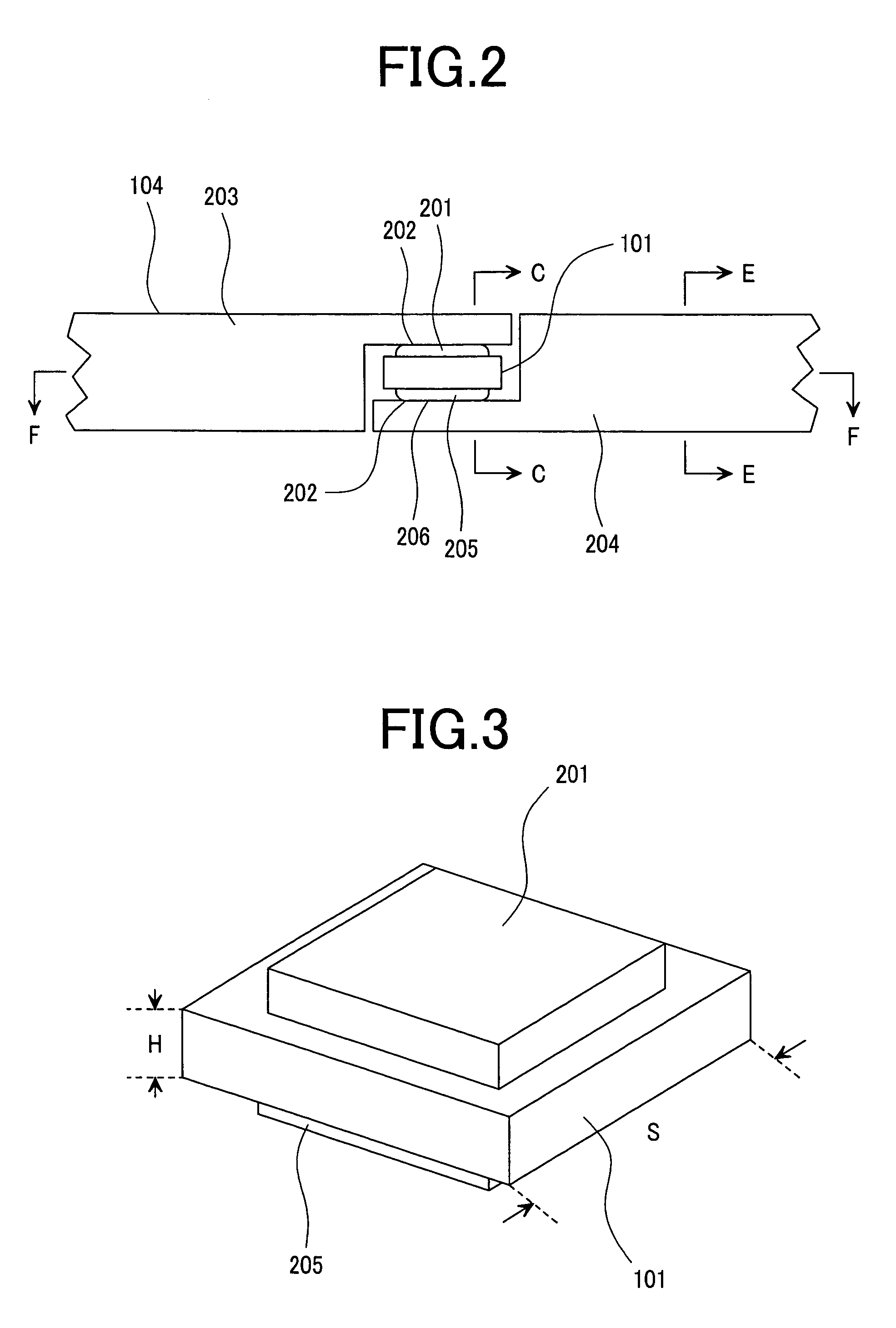
[0051]FIG. 1 is a perspective view showing an enlarged connection part of an IC tag chip in the first embodiment of the present invention and an antenna. FIG. 2 shows FIG. 1 when viewed from symbol B, and shows a section of a portion in which the IC tag chip and the antenna are connected. FIG. 3 shows a perspective view of the IC tag chip of FIG. 1. A section taken along a line C-C of FIG. 2 is shown in FIG. 4A, which shows a section of the wireless IC tag in the IC tag chip portion. FIG. 4B shows a section taken along a line E-E of FIG. 2. FIG. 5A shows a section taken along a line F-F of FIG. 2. FIG. 5B is an explanatory drawing on manufacturing.

[0052]Hereinafter, detailed descriptions will be given.

[0053]The wireless IC tag 104 of the present invention comprises an IC tag chip 101 and a pair of antenna conductors 203 and 204 with circular sections connected to its electrodes. The p...

second embodiment

[0107]FIG. 14 shows a wireless IC tag of another embodiment of the present invention. The drawing shows the sectional view of a portion in which an IC tag chip and an antenna are connected. In this embodiment, the wireless IC tag 104 comprises an IC tag chip 101 and a pair of antenna conductors 203 and 204 with a circular section, connected to the electrodes of the IC tag chip 101. The pair of antenna conductors extends in an axial direction with the IC tag chip 10 sandwiched, and constitutes a dipole antenna with a narrow width. The bumps 201 and 205 are on the upper face and the lower face of the IC tag chip 101, respectively, and exist on both sides of the IC tag chip. The bumps are connected to the antennas 203 and 204. The antennas may have a rectangular or elliptical section. The maximum width of the antennas is equal to the maximum value defined in the case of projection, and its maximum value is 1.0 mm or less and its minimum value is one micron or more.

[0108]In this structu...

third embodiment

[0109]FIG. 15 shows a wireless IC tag according to another embodiment of the present invention. The drawing shows the sectional view of a portion in which an IC tag chip and an antenna are connected. In this embodiment, the wireless IC tag 104 comprises an IC tag chip 101 and a pair of antenna conductors 203 and 204 with a circular section, connected to the electrodes of the IC tag chip 101. The pair of antenna conductors extends in an axial direction with the IC tag chip 101 sandwiched, and constitutes a dipole antenna with an arrow width. The antennas 203 and 204 having antenna hooks 208 are connected to the bumps with the bumps 201 and 205 on the upper side and the lower side of the IC tag chip 101 and on both sides of the IC tag chip. The antennas may have a rectangular or elliptical section. The maximum width of the antennas is equal to the maximum value defined in the case of projection, and its maximum value is 1.0 mm or less and its minimum value is one micron or more.

[0110]...


PUM


Abstract

There is a problem related to radio wave interference, e.g. the shade of radio wave of a radio IC tag, when a plurality of radio IC tags are present in a region of electromagnetic wave. When a plurality of antennas each having a large area are present in the vicinity of the radio IC tag, the radio IC tag easily receives the affect of an antenna conductor. In a plurality of radio IC tags present in a radio wave area, width of the antenna conductor of the radio IC tag is set at 1.0 mm or less. Furthermore, in order to realize an antenna conductor having a small width, an IC tag chip of both side electrode structure having electrodes on the front surface and rear surface of a chip is sandwiched between antennas.

Description

TECHNICAL FIELD[0001]The present invention relates to a wireless IC tag wirelessly identified and a process of manufacturing the same, and more particularly to a wireless IC tag having a congestion control function and a process for manufacturing the same.BACKGROUND ART[0002]A wireless IC tag has identification information about a product or the like to which it is adhered, and by reading the identification information, is used for widespread application such as is read for stock control, product inspection, and history management. For example, the wireless IC tags are used to individually identify and manage a large number of cartridge products housed in a carton. In this case, even when two products are close to each other, to correctly identify them by IC tags, wireless IC tags tolerant of radio wave interference are required.[0003]As an example of wireless IC tags tolerant of radio wave interference, technology disclosed in Japanese Patent Laid-Open No. H11-53492 exists. In this...

Claims


Application Information

Patent Timeline
Patent Type & Authority Patents(United States)
IPC IPC(8): G08B13/14H01Q1/22H01Q9/16
CPCG06K19/0775H01Q1/22H01Q9/16H01L2224/16227H01L2924/07811H01L2224/16225H01L2924/00
Inventor USAMI, MITSUO
Owner HITACHI LTD
Why Eureka
Try Eureka