Silicon germanium heterostructure barrier varactor

a heterostructure varactor and silicon germanium technology, applied in the field of semiconductor heterostructure barrier (hbv) diodes, can solve the problems of reducing the overall efficiency of this type of multiplier circuit, reducing the quality of the diode, and limited chemistry of the use of heterostructure varactors

Inactive Publication Date: 2010-04-13
IBM CORP
View PDF23 Cites 4 Cited by
  • Summary
  • Abstract
  • Description
  • Claims
  • Application Information

AI Technical Summary

Benefits of technology

[0007]Bearing in mind the problems and deficiencies of the prior art, it is therefore an object of the present invention to provide easy and efficient methods of making barrier varactors in silicon technology and the resultant barrier varactors made thereby.
[0009]A further object of the invention is to provide methods and heterostructure barrier varactors integrated into silicon-based technology to enable silicon monolithic microwave integrated circuits having improved performance.

Problems solved by technology

However, Schottky diodes unfortunately create harmonics at both even and odd frequencies, thereby reducing the overall efficiency of this type of multiplier circuit.
Conventional P-N junction diodes and Schottky diodes are also plagued by the presence of leakage current, which lowers the quality of the diode.
However, the use of heterostructure varactors is limited in its chemistry, and has yet to be easily and efficiently extended into silicon technology.

Method used


Image

  • Silicon germanium heterostructure barrier varactor
  • Silicon germanium heterostructure barrier varactor
  • Silicon germanium heterostructure barrier varactor

Examples


Embodiment Construction

)

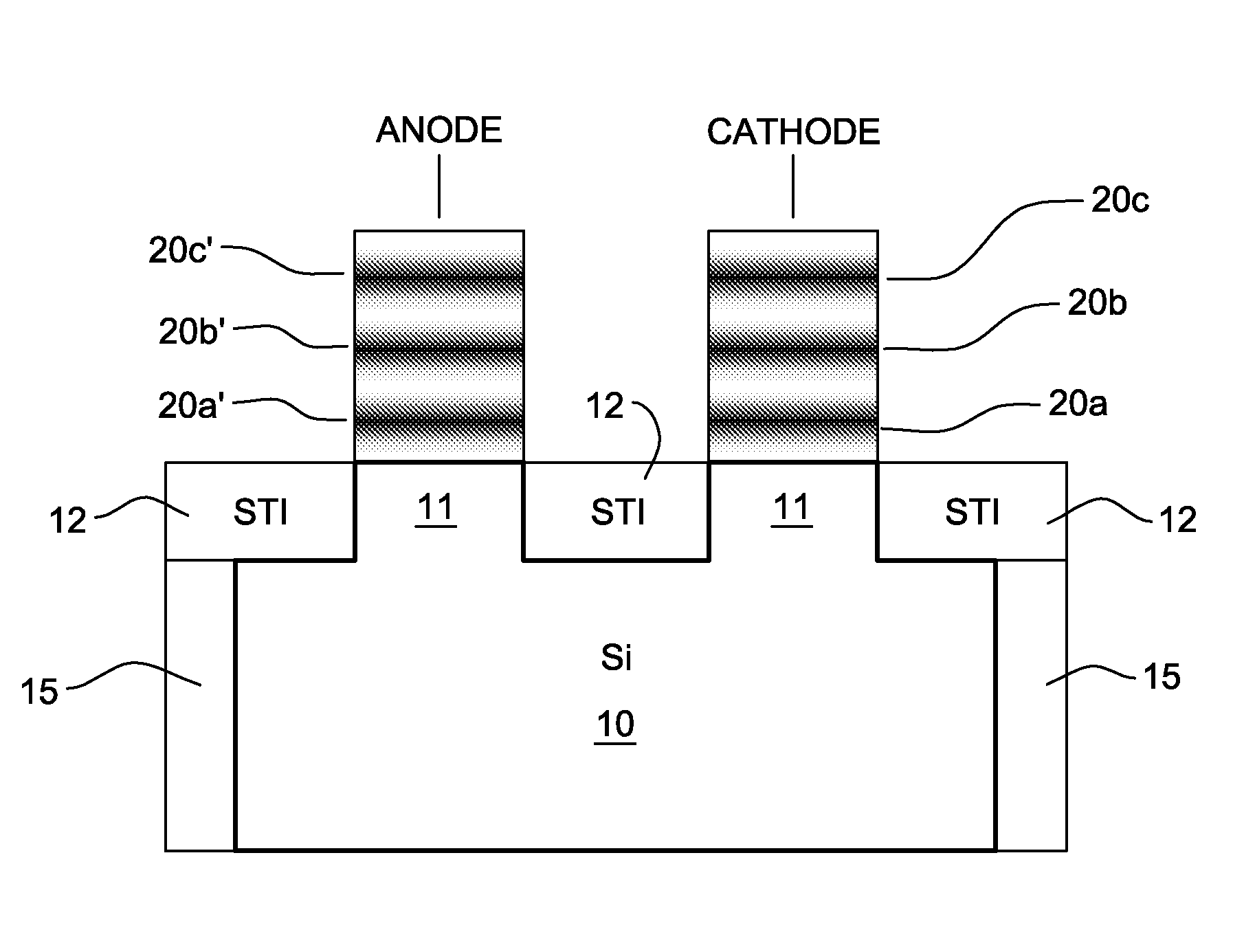
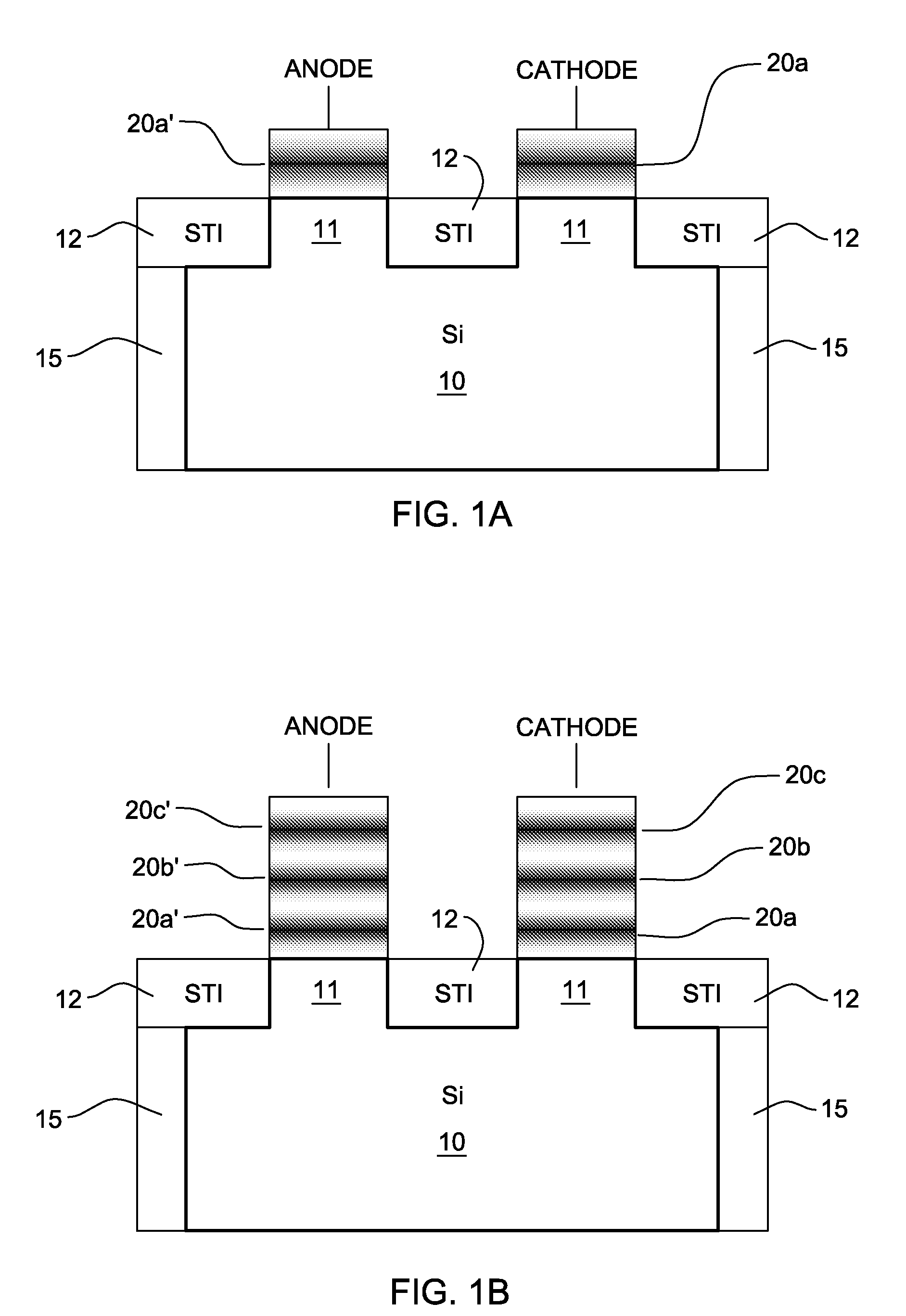
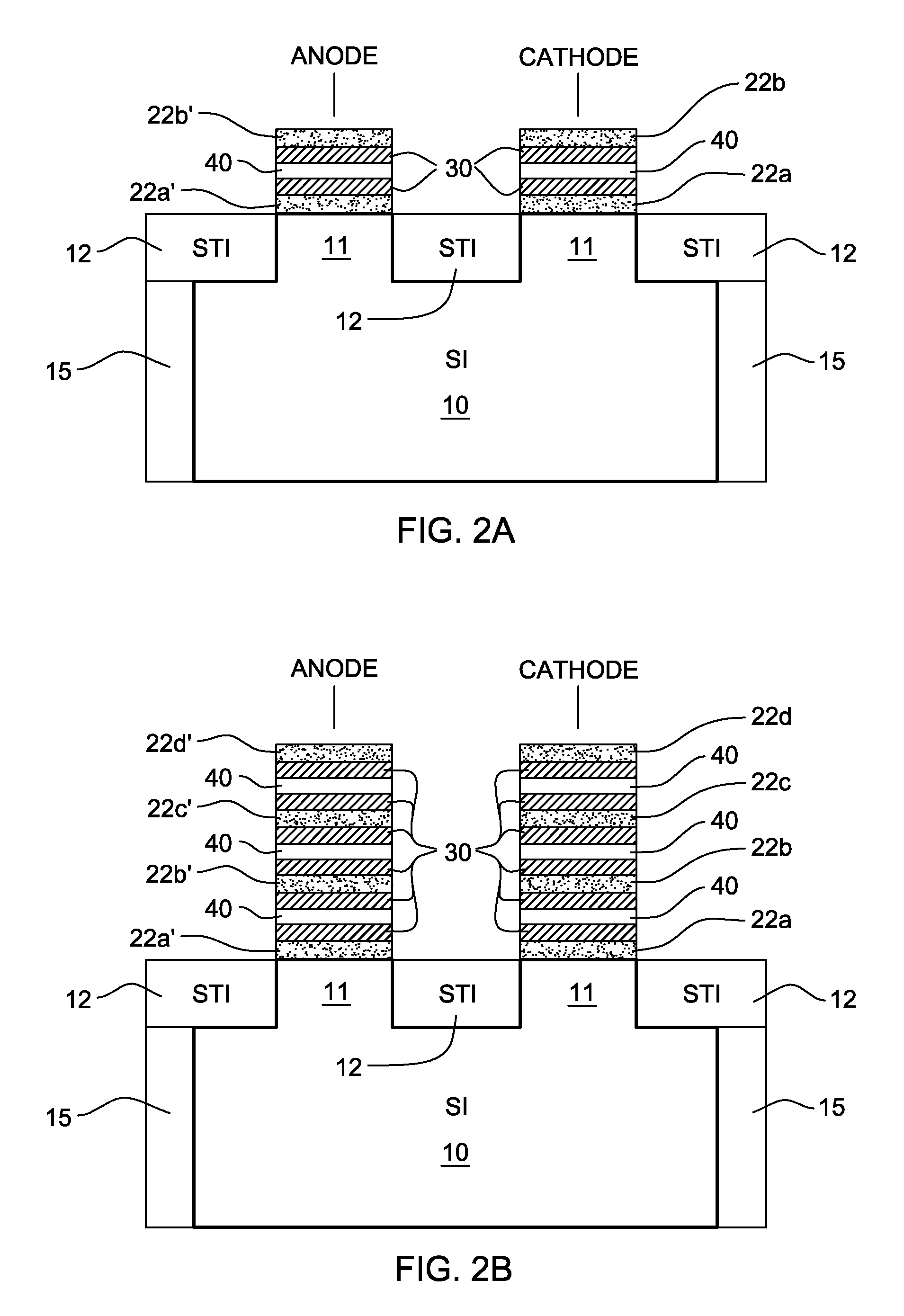
[0026]In describing the preferred embodiment of the present invention, reference will be made herein to FIGS. 1A-6B of the drawings in which like numerals refer to like features of the invention.

[0027]The present invention is directed to novel heterostructure barrier varactor (HBV) diodes on silicon-containing substrates that provide silicon monolithic microwave integrated circuits with significantly improved performance. The present HBV diodes are silicon / silicon germanium (Si / SiGe) quantum well HBVs suitable for use as frequency multipliers at submillimeter wave frequencies and above.

[0028]Referring to the drawings, a silicon or silicon-containing layer or substrate 10 (hereinafter referred to as silicon layer 10) is provided over a semiconductor substrate 5. The silicon layer 10 may be a p-type material or an n-type material. Shallow trench isolation regions (STI) 12, such as STI oxide regions, are formed by known techniques to isolate adjacent p-type silicon regions 11 from one...


PUM


Abstract

Methods and heterostructure barrier varactor (HBV) diodes optimized for application with frequency multipliers at providing outputs at submillimeter wave frequencies and above. The HBV diodes include a silicon-containing substrate, an electrode over the silicon-containing substrate, and one or more heterojunction quantum wells of alternating layers of Si and SiGe of one or more electrodes of the diode. Each SiGe quantum well preferably has a floating SiGe layer between adjacent SiGe gradients followed by adjacent Si layers, such that, a single homogeneous structure is provided characterized by having no distinct separations. The plurality of Si / SiGe heterojunction quantum wells may be symmetric or asymmetric.

Description

FIELD OF THE INVENTION[0001]The present invention relates to semiconductors devices and, more particularly, to semiconductor heterostructure barrier (HBV) diodes.DESCRIPTION OF RELATED ART[0002]Semiconductor devices known as varactor diodes are characterized as having a capacitance that varies as a variable bias voltage is applied to a depletion region of the diode. That is, as a reverse voltage is applied to a PN junction of the varactor diode, electrons in the n-region are attracted to the cathode while holes in the p-region are attracted to the anode. The result is a depletion region between the anode and cathode that behaves as the dielectric of the device. As the applied reverse voltage increases, the depletion region (i.e., dielectric) widens, while the capacitance across the PN junction decreases since capacitance is inversely proportional to dielectric thickness. Therefore, by varying the reverse voltage across a PN junction of a varactor diode, the junction capacitance can ...

Claims


Application Information

Patent Timeline
Patent Type & Authority Patents(United States)
IPC IPC(8): H01L29/93H01L27/108H01L29/76H01L29/94H01L31/119
CPCH01L29/155H01L29/93H01L29/165
Inventor DAHLSTROM, ERIK M.JOSEPH, ALVIN J.RASSEL, ROBERT M.SHERIDAN, DAVID C.
Owner IBM CORP
Why Eureka
Try Eureka