Power control circuitry and method

a power control circuit and circuit technology, applied in logic circuits, high-tension/heavy-dress switches, electric variable regulation, etc., can solve the problems of circuits that can consume significant power, circuits that are not easy to operate, and many circuits within the system spend a significant proportion of the time inactive, etc., to achieve the effect of simplifying logi

Active Publication Date: 2010-04-13
ARM LTD
View PDF4 Cites 21 Cited by
  • Summary
  • Abstract
  • Description
  • Claims
  • Application Information

AI Technical Summary

Benefits of technology

[0016]By such an approach, the turning on of the various power switching circuits can be staggered so as to limit the peak current, and accordingly reduce inrush current that might otherwise occur if all of the power switching circuits were turned on at the same time. Since the enable qualifying circuit only sets its output signal when the associated power switching circuit has been enabled and the charging function achieved by that power switching circuit has caused the voltage level on the relevant voltage line(s) to reach a predetermined voltage level, then this enables the enable signal provided to a later power switching circuit in the series to only be set once that predetermined voltage level has been achieved in a circuit portion associated with an earlier power switching circuit (i.e. the power switching circuit with which the enable qualifying circuit is associated). By controlling the setting of the enable signals in such a manner, then the staggering of the setting of the enable signals can be achieved in a manner which is independent of process variation in the components of the power control circuitry. Furthermore, the enable qualifying circuit can be readily provided by simple digital components, thereby significantly reducing the area and hence cost when compared with complex analog solutions that seek to reduce inrush current.
[0024]In addition to the output signal generating component, the enable qualifying circuit may include one or more further components dependent on the implementation. For example, in one embodiment, each enable qualifying circuit further comprises inverter logic for inverting at least one of the enable signal and the voltage level signal prior to supply to the first input or second input, respectively, of the output signal generating component. By appropriate use of inverters, this can simplify the logic required in the output signal generating component.

Problems solved by technology

In a data processing system, it is often the case that many of the circuits within the system spend a significant proportion of the time inactive.
However, even when inactive, those circuits can consume significant power due to leakage current.
Irrespective of whether the circuit of any particular implementation requires any data holding mechanisms such as the above-mentioned diode mechanism in order to allow the circuit to hold data values whilst it is in the standby mode, a common problem that can occur in any circuit employing power control circuitry is a problem of inrush current when the circuit is later re-connected to the voltage source.
A large inrush current (voltage surge) may occur in the power supply VDD during this charging period, and this large inrush current may cause voltage drops in the power supply VDD, which might potentially cause other circuits using the power supply VDD to malfunction.
In particular, any variations in the ground voltage line may again cause other circuits to malfunction.
However, whilst such an approach can limit the peak current, and thereby reduce the inrush current, the approach of using simple circuits such as a weak driver to reduce the slew rate of the power switch enable signal provided to the gates of the power switches is very sensitive to manufacturing process variations, and accordingly the amount of current limitation that can be achieved will vary significantly dependent on such process variations.
As a result, such an approach does not provide a very reliable technique for reducing inrush current.
Whilst the use of more complex analog circuits such as the above-mentioned charge pumps can remove some of the process sensitivity that would be exhibited by the earlier-mentioned technique for limiting the slew rate of the enable signals provided to the power switch gates, their increased complexity adds to the area of the power control circuitry which in turn increases cost.

Method used


Image

  • Power control circuitry and method
  • Power control circuitry and method
  • Power control circuitry and method

Examples


third embodiment

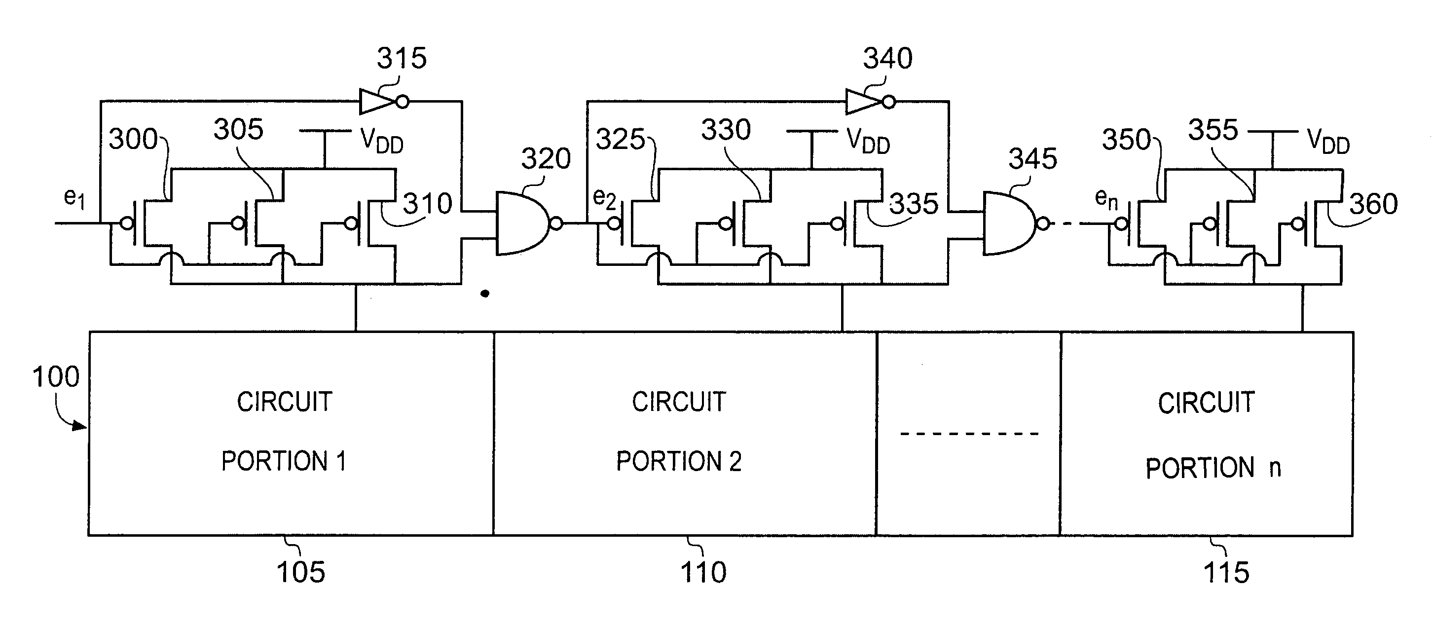
[0052]Whilst in FIGS. 3 and 4, the various switching circuits have been considered to consist of a single transistor, in alternative embodiments the switching circuits may take different forms. For example, FIG. 5 shows a third embodiment which is analogous to the earlier embodiment described with reference to FIG. 3, but in this case each of the single transistors 200, 215, 230 of FIG. 3 have been replaced with three PMOS transistors in parallel 300, 305, 310, 325, 330, 335, and 350, 355, 360, respectively. The inverters 315, 340 and NAND gates 320, 345 operate in an identical manner to the inverters 205, 220 and NAND gates 210, 225 of FIG. 3. By using multiple transistors in parallel, the switching circuits may be arranged to pull the internal voltage line(s) within the associated circuit portions up towards the operating supply voltage VDD more quickly, assuming similar strength PMOS transistors are used in the embodiment of FIG. 5 to those used in the embodiment of FIG. 3. The u...

first embodiment

[0053]FIGS. 6A to 6D illustrate alternative forms of switching circuit and associated enable qualifying circuit that may be used instead of the arrangement of FIG. 3. Hence, considering FIG. 6A, the PMOS transistor 400, inverter 405 and NAND gate 410 operate in an identical manner to the elements 200, 205, 210, or 215, 220, 225 of FIG. 3. However, in this example, delay circuitry 420 is provided in association with the second input to the NAND gate 410 to increase the predetermined voltage level that must be reached before the output from the NAND gate 410 is set. In this particular example, the delay circuitry takes the form of a sequence of inverters, but it will be appreciated that alternative circuitry could be used instead of inverters to achieve the same effect of delaying the second input to the NAND gate 410.

[0054]FIG. 6B illustrates an alternative embodiment where the inverter is provided in association with the second input rather than the first input as shown in FIG. 3. A...


PUM


Abstract

The power control circuitry comprises a series of power switching circuits, each power switching circuit being associated with one of the circuit portions and being provided with an enable signal and responsive to its enable signal being set to connect the voltage source to the at least one voltage line of the associated circuit portion. Further, at least one enable qualifying circuit is provided, each such enable qualifying circuit being associated with one of the power switching circuits and being arranged to generate an output signal used to determine the enable signal provided to a later power switching circuit in the series. Each enable qualifying circuit sets its output signal when both the enable signal provided to the associated power switching circuit is set and the at least one voltage line of the circuit portion associated with that power switching circuit has reached a predetermined voltage level.

Description

BACKGROUND OF THE INVENTION[0001]1. Field of the Invention[0002]The present invention relates to power control circuitry, and to a method of operating such circuitry, such power control circuitry being arranged to control the connection of a voltage source to an associated circuit.[0003]2. Description of the Prior Art[0004]In a data processing system, it is often the case that many of the circuits within the system spend a significant proportion of the time inactive. However, even when inactive, those circuits can consume significant power due to leakage current. Accordingly, it is known to provide power control circuitry in association with such circuits to disconnect those circuits from a voltage source when they are not being used, and to then reconnect them to the voltage source when those circuits need again to become active.[0005]FIG. 1 is a schematic diagram illustrating a known power control circuitry that can be provided in association with a circuit 40. In this example, th...

Claims


Application Information

Patent Timeline
Patent Type & Authority Patents(United States)
IPC IPC(8): H01H7/00H01H9/54
CPCH03K17/28H03K19/0016H03K17/30
Inventor FREY, CHRISTOPHESOWDEN, ANDREW JOHN
Owner ARM LTD
Why Eureka
Try Eureka