Chip coated light emitting diode package and manufacturing method thereof

a technology of light-emitting diodes and manufacturing methods, which is applied in the manufacturing of semiconductor/solid-state devices, semiconductor devices, electrical devices, etc., can solve the problems of limiting the miniaturization of the package, affecting the reliability of the package, and not uniform color temperature, so as to prevent color temperature differences, improve light efficiency, and increase yield

Active Publication Date: 2010-05-11
SAMSUNG ELECTRONICS CO LTD
View PDF2 Cites 42 Cited by
  • Summary
  • Abstract
  • Description
  • Claims
  • Application Information

AI Technical Summary

Benefits of technology

[0017]The present invention has been made to solve the foregoing problems of the prior art and therefore an aspect of the present invention is to provide a chip coated Light Emitting Diode (LED) package which can improve light efficiency by preventing differences in color temperature according to irradiation angles, increase a yield, and allows miniaturization and accommodate mass production, and a manufacturing method thereof.

Problems solved by technology

This adversely causes non-uniform color temperature according to the irradiation angles of white light.
Thus, made of heavy metal-based powder having electric conductivity, the YAG-based, TAG-based and Silicate-based fluorescent material may cause leakage current degrading the light efficiency of the light emitting chip 14 during light emission, ultimately undermining the reliability of the package.
This limits miniaturization of the package, complicates the manufacturing process and increases the manufacturing costs.

Method used


Image

  • Chip coated light emitting diode package and manufacturing method thereof
  • Chip coated light emitting diode package and manufacturing method thereof
  • Chip coated light emitting diode package and manufacturing method thereof

Examples


first embodiment

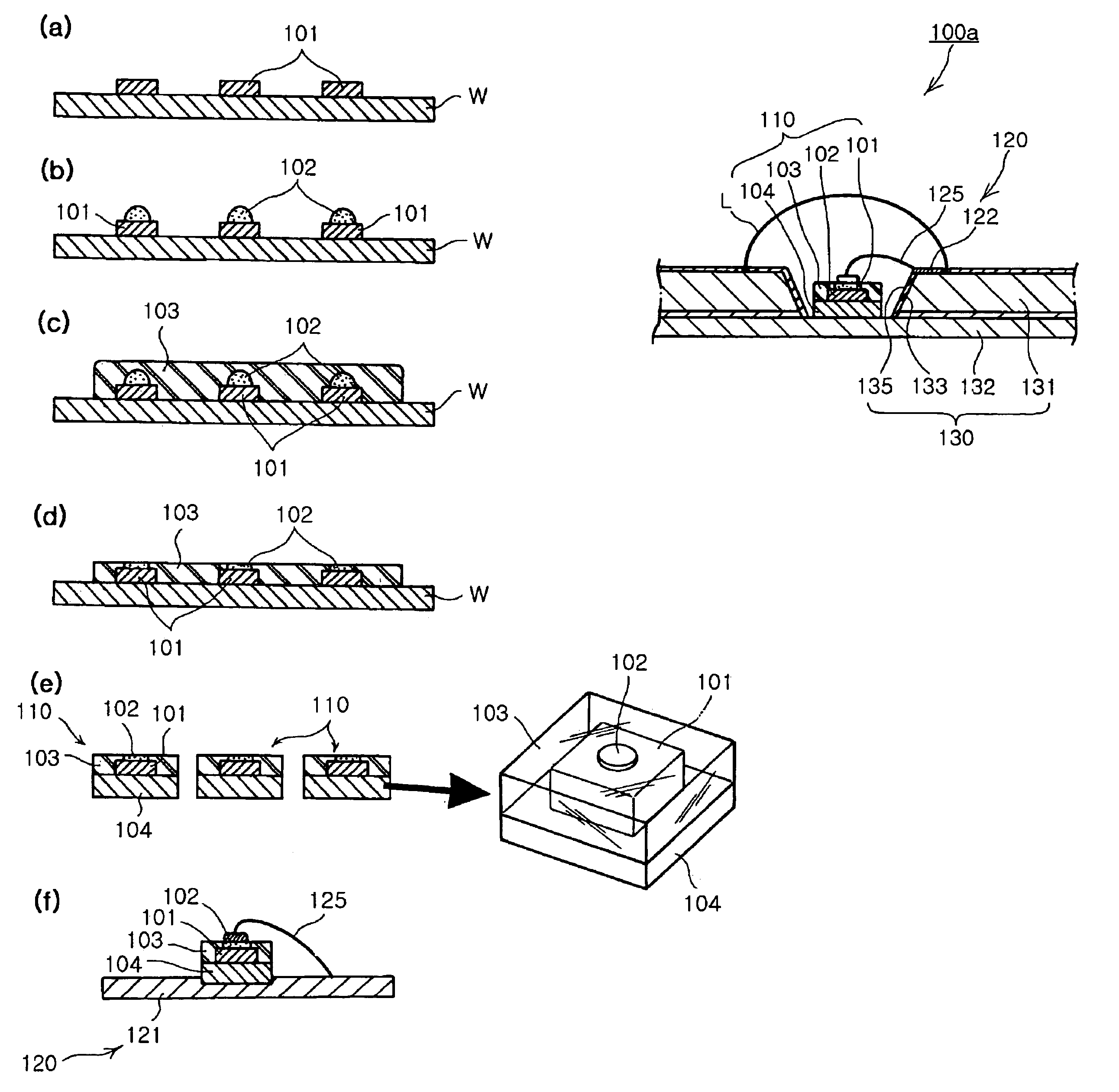
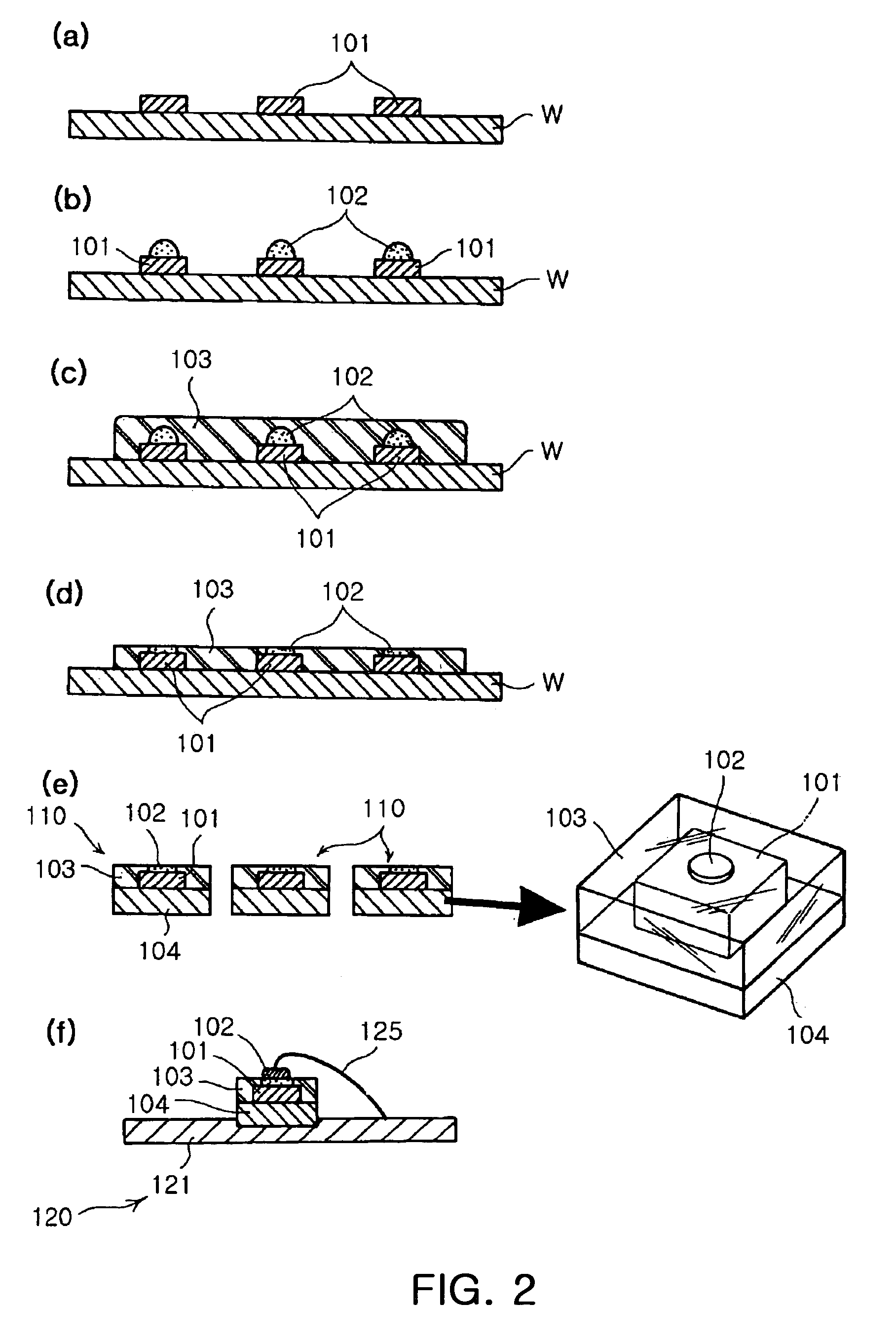
[0038]FIG. 2(a) to (f) is a view illustrating the fabrication of a chip coated LED package according to the present invention and FIG. 3 is a perspective view illustrating a chip coated LED package according to the present invention.

[0039]The LED package 100 according to the present invention includes a light emitting chip 110, an electrode part 120 and a package body 130.

[0040]The light emitting chip 110 includes a chip die 101, a bump ball 102, a resin layer 103 and a submount 104. The chip die 101, which is die-attached on the submount 104, is a light emitting source for generating light when power is applied.

[0041]Here, the chip die 101 is a light emitting source for generating near ultraviolet rays or blue light when power is applied. For such a chip die 101, it is preferable to use a gallium nitride-based light emitting diode chip which generates blue light with high output and high luminance. The chip die 101 can adopt a horizontal structure in which both p- and n-electrodes ...

second embodiment

[0053]In the meantime, FIG. 4 illustrates a chip coated LED package according to the present invention. In this embodiment, the package body 130 of the LED package 100a may include a metal chassis 132 with the light emitting chip 110 mounted thereon and a substrate 131 having a predetermined dimension of disposition hole 133 for exposing the light emitting chip 110 and having the electrode part 120 pattern printed on an upper surface thereof.

[0054]Here, the disposition hole 133 may also have a reflecting part 135 for reflecting the light generated from the light emitting chip 110.

[0055]In addition, the package body 130 provided in the form of a substrate can also have a lens L provided on an upper part thereof in order to widen the beam angle of light generated from the light emitting chip 110 or increase the light efficiency. A filler made of a transparent resin is filled in the space of the disposition hole 133 enclosed by the lens L.

[0056]As shown in FIG. 2(a), a manufacturing me...


PUM


Abstract

A chip coated LED package and a manufacturing method thereof. The chip coated LED package includes a light emitting chip composed of a chip die-attached on a submount and a resin layer uniformly covering an outer surface of the chip die. The chip coated LED package also includes an electrode part electrically connected by metal wires with at least one bump ball exposed through an upper surface of the resin layer. The chip coated LED package further includes a package body having the electrode part and the light emitting chip mounted thereon. The invention improves light efficiency by preventing difference in color temperature according to irradiation angles, increases a yield, miniaturizes the package, and accommodates mass production.

Description

CLAIM OF PRIORITY[0001]This application claims the benefit of Korean Patent Application No. 2006-0002829 filed on Jan. 10, 2006, in the Korean Intellectual Property Office, the disclosure of which is incorporated herein by reference.BACKGROUND OF THE INVENTION[0002]1. Field of the Invention[0003]The present invention relates to a chip coated Light Emitting Diode (LED) package and a manufacturing method thereof and, more particularly, to a chip coated LED package which increases light extraction efficiency, accommodates miniaturization of a product and reduces manufacturing costs, and to a manufacturing method thereof.[0004]2. Description of the Related Art[0005]In general, a Light Emitting Diode (hereinafter referred to as ‘LED’) is an electric component which converts electric energy to light energy from recombination of minority carriers (electrons and holes) injected through a p-n junction structure of semiconductor and thereby emits the light. That is, when a forward voltage is ...

Claims


Application Information

Patent Timeline
Patent Type & Authority Patents(United States)
IPC IPC(8): H01L33/00H01L21/00H01L33/44H01L33/50H01L33/58H01L33/62
CPCH01L33/62H01L33/508H01L2924/01079H01L2924/01078H01L2224/48465H01L2224/48257H01L2224/48247H01L2224/48091H01L2924/00014H01L2924/00
Inventor LEE, SEON GOOHAN, KYUNG TAEGHAN, SEONG YEON
Owner SAMSUNG ELECTRONICS CO LTD
Why Eureka
Try Eureka