
Hetero junction semiconductor device

a semiconductor device and heteroconductor technology, applied in the field of heteroconductor devices, can solve the problems of increasing resistance, failing to sufficiently effect a good inherent feature of the device, and difficult to protect the gate insulating film, etc., and achieves low resistance and high voltage capability.

Active Publication Date: 2010-05-11
NISSAN MOTOR CO LTD
View PDF19 Cites 16 Cited by
  • Summary
  • Abstract
  • Description
  • Claims
  • Application Information

AI Technical Summary

Benefits of technology

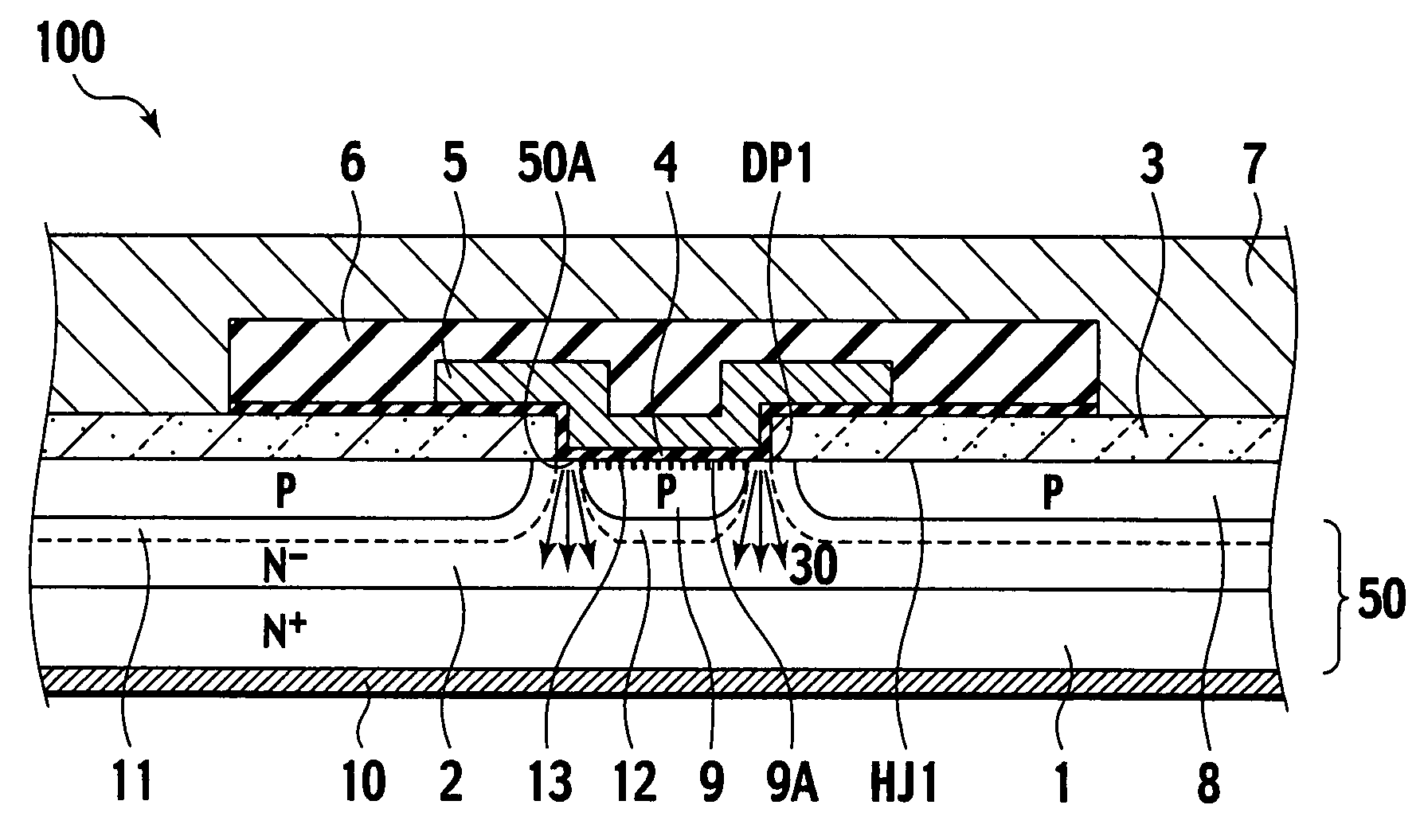
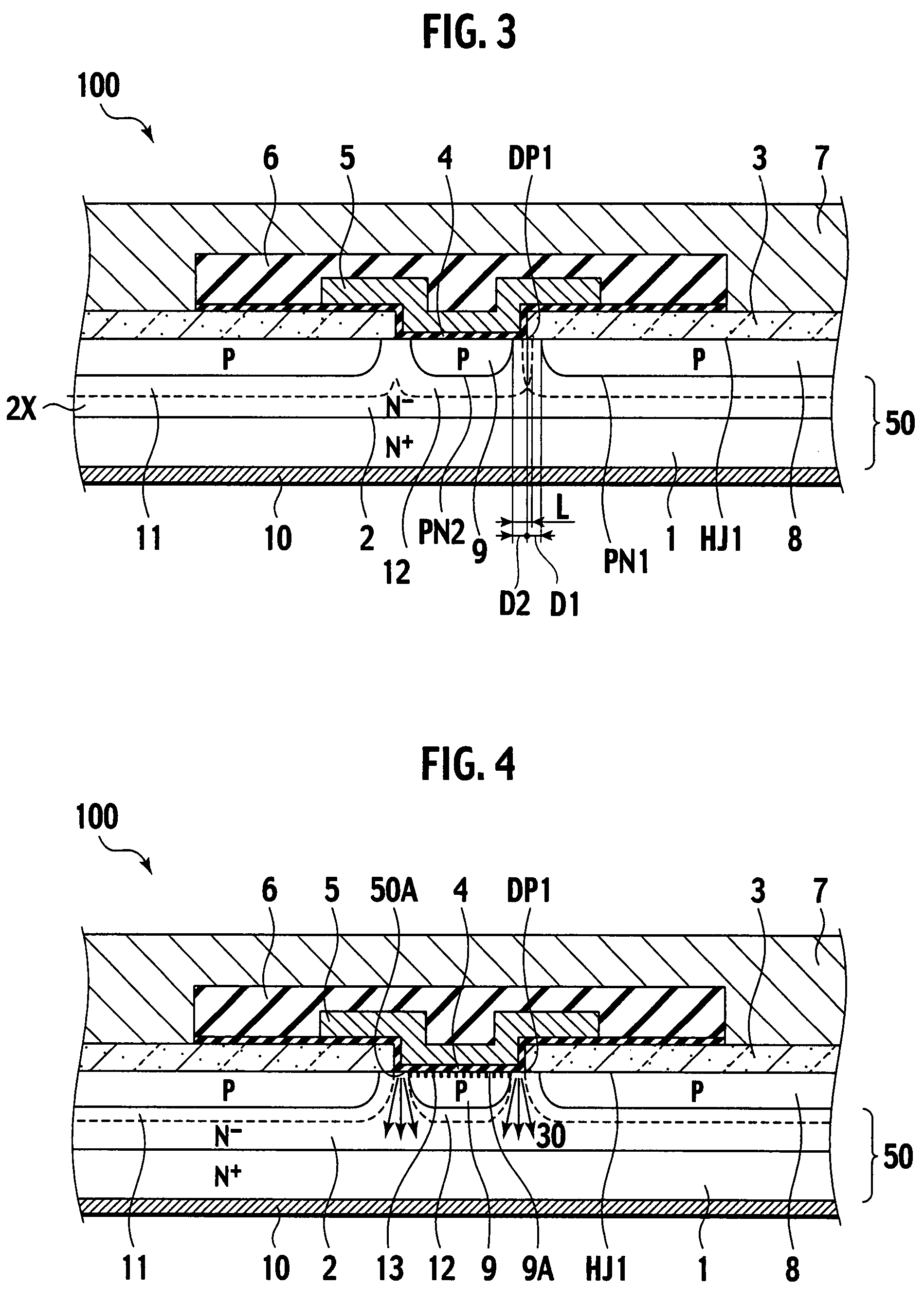
The proposed structure effectively relaxes the field when the device is off, while forming an inversion layer when on, thereby improving the trade-off between off-state protection and on-state current passage, achieving high reverse blocking voltage and low on-resistance.

Problems solved by technology

Without connecting the P type region's potential to a source potential, however, the above field relaxing effect is restrictive, thus making it difficult to protect the gate insulating film.
With the above structure, sufficiently implementing the field relaxing when the element is off may narrow a current passage when the element is on, thus increasing an on-resistance, which is a trade off, failing to sufficiently effect a good inherent feature of the device.

Method used


Image

  • Hetero junction semiconductor device
  • Hetero junction semiconductor device
  • Hetero junction semiconductor device

Examples


first embodiment

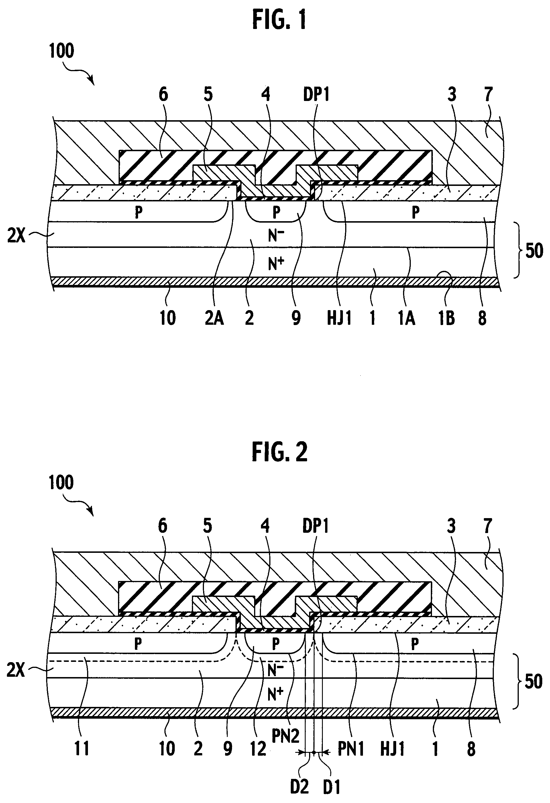
[0025]Referring to FIG. 1 to FIG. 6, a semiconductor device 100 is to be set forth, according to the first embodiment of the present invention.

[0026]FIG. 1 shows a cross sectional structure of a field effect transistor device which is the semiconductor device 100 under the present invention. In the above cross section, two unit cells are oppositely arranged. Actually however, a plurality of the unit cells are connected in parallel, thus forming the field effect transistor. The description is to be made, however, based on the above typical cross sectional structure.

[0027]At first, in terms of structure, there is provided an N+ type SiC substrate region 1, with the superscript “+” denoting a high concentration. The N+ type SiC substrate region 1 has a first face 1A on which an N− type SiC drain region 2 is formed, with the superscript “−” denoting a low concentration. The drain region 2 includes an epitaxial layer 2X grown on the SiC substrate region 1. A semiconductor substrate 50 ha...

second embodiment

[0046]Referring to FIG. 7, the semiconductor device 100 is to be set forth, according to the second embodiment of the present invention.

[0047]The semiconductor device 100 has such a structure that a slit part 33 is formed in the N− type SiC drain region 2 below the hetero semiconductor region 3, with a P+ type hetero semiconductor 18 embedded in the slit part 33. By way of a connection part 19 made of P+ type hetero semiconductor, the P+ type hetero semiconductor 18 connects to the source electrode 7.

[0048]With the above structure, the barrier height of a hetero junction HJ2 (hetero interface) formed between the P+ type hetero semiconductor 18 and the N− type SiC drain region 2 is larger than in the case of the N type hetero semiconductor, thereby bringing about a junction featuring lower leak and higher voltage capability. A depletion layer (not shown in FIG. 7) from the above hetero junction HJ2 (hetero interface) expands, thereby bringing about an effect of suppressing an opposit...

third embodiment

[0052]Referring to FIG. 8, the semiconductor device 100 is to be set forth, according to the third embodiment of the present invention.

[0053]The semiconductor device 100 has such a structure that a slit part 66 is formed in the N− type SiC drain region 2 below the hetero semiconductor region 3, with a Schottky electrode 20 embedded in the slit part 66.

[0054]With the above structure, a depletion layer (not shown in FIG. 8) from the Schottky electrode 20 (Schottky interface) expands, thereby bringing about an effect of suppressing the opposite leak current, together with the effect brought about by the depletion layer (not shown in FIG. 8) from the field relaxing region 9 below the gate electrode 5.

[0055]The property of the element when the element is on according to the third embodiment is equivalent to that according to the first embodiment.

[0056]Set forth below is a production method according to the third embodiment.

[0057]Specifically, a dry etching and the like is used for formin...


PUM


Abstract

A semiconductor device, includes: a first conductivity-semiconductor substrate; a hetero semiconductor region for forming a hetero junction with the first conductivity-semiconductor substrate; a gate electrode adjacent to a part of the hetero junction by way of a gate insulating film; a drain electrode connecting to the first conductivity-semiconductor substrate; a source electrode connecting to the hetero semiconductor region; and a second conductivity-semiconductor region formed on a part of a first face of the first conductivity-semiconductor substrate in such a configuration as to oppose the gate electrode via the gate insulating film, the gate insulating film, the hetero semiconductor region and the first conductivity-semiconductor substrate contacting each other to thereby form a triple contact point. A first face of the second conductivity-semiconductor region has such an impurity concentration that allows a field from the gate electrode to form an inversion layer on the first face of the second conductivity-semiconductor region.

Description

BACKGROUND OF THE INVENTION[0001]1. Field of the Invention[0002]The present invention relates to a semiconductor device.[0003]2. Description of the Related Art[0004]Japanese Patent Application Laid-Open No. JP2003-318398 (=JP2003318398) discloses a silicon carbide semiconductor device, specifically, a field effect transistor using a hetero interface. According to the above related art, a voltage applied to a gate electrode controls thickness of a barrier at the hetero interface, and a tunnel current allows a carrier to pass by when an element is on. In this case, a channel region such as MOSFET is not present, thereby providing a power semiconductor switch having high voltage capability (high reverse blocking voltage) and low on-resistance.[0005]The above related art has such a structure that a P type region is formed on the gate electrode and on a silicon carbide SiC region below the gate electrode, thereby relaxing a field applied to a gate insulating film. Without connecting the ...

Claims


Application Information

Patent Timeline
Patent Type & Authority Patents(United States)
IPC IPC(8): H01L31/0312H01L29/10H01L31/036H01L29/93
CPCH01L29/0619H01L29/7828H01L29/267H01L29/66068H01L29/0623H01L29/0696H01L29/1608
Inventor SHIMOIDA, YOSHIOHOSHI, MASAKATSUHAYASHI, TETSUYATANAKA, HIDEAKIYAMAGAMI, SHIGEHARU
Owner NISSAN MOTOR CO LTD
Learn More