Nanoeletromechanical switch and logic circuits formed therefrom

a technology of logic circuits and switches, applied in nanoelectromechanical switches, pulse techniques, instruments, etc., can solve problems such as extreme low leakage curren

Active Publication Date: 2010-05-18
NAT TECH & ENG SOLUTIONS OF SANDIA LLC
View PDF6 Cites 30 Cited by
  • Summary
  • Abstract
  • Description
  • Claims
  • Application Information

AI Technical Summary

Benefits of technology

[0021]The voltage provided to one of the two pairs of gate electrodes in each NEM switching device can provide a logic state input to that NEM switching device; and the voltage provided to the other of the two pairs of gate electrodes in each NEM switching device can provide a disable input to that NEM switching device. The voltage for the logic state input can either be the same or different from the voltage for the disable input. The disable input is useful to render that NEM switching device unresponsive to the logic state input.
[0022]The digital logic circuit can include one or more NAND gates formed from the plurality of interconnected NEM switching devices. Each NAND gate can have a plurality of logic state inputs and a plurality of disable inputs to provide an output which is determined by a NAND function of the logic state inputs when the disable inputs are in a first logic state, with the output being electrically floating or tied to a power supply voltage (e.g. Vss) when the disable inputs are in a second logic state. Alternately, or in addition to the NAND gates, the digital logic circuit can include one more NOR gates formed from the plurality of interconnected NEM switching devices. Each NOR gate can have a plurality of logic state inputs and a plurality of disable inputs to provide an output which is determined by a NOR function of the logic state inputs when the disable inputs are in a first logic state, with the output being electrically floating or tied to a power supply voltage (e.g. Vdd) when the disable inputs are in a second logic state.
[0023]In some embodiments of the present invention, the digital logic circuit can include one or more programmable logic gates which can be switched between different types of logic functions (e.g. between a NAND logic function and a NOR logic function). This can be done using a pair of the NEM switching devices to switch power supply connections to the programmable logic gates.
[0024]The digital logic circuit formed according to the present invention can also include one or more SRAM memory cells which are formed, at least in part, from the plurality of interconnected NEM switching devices.
[0025]The digital logic circuit of the present invention can also include one or more cross-coupled data latches formed from the plurality of interconnected NEM switching devices. Each cross-coupled data latch can be used, for example, to form a core of a SRAM memory cell.

Problems solved by technology

Removing the gate voltage from the NEM switching device interrupts the electrical connection between the source and drain electrodes, thereby resulting in an extremely low leakage current which is due to Brownian motion of the cantilever arm and tunneling.

Method used


Image

  • Nanoeletromechanical switch and logic circuits formed therefrom
  • Nanoeletromechanical switch and logic circuits formed therefrom
  • Nanoeletromechanical switch and logic circuits formed therefrom

Examples


Embodiment Construction

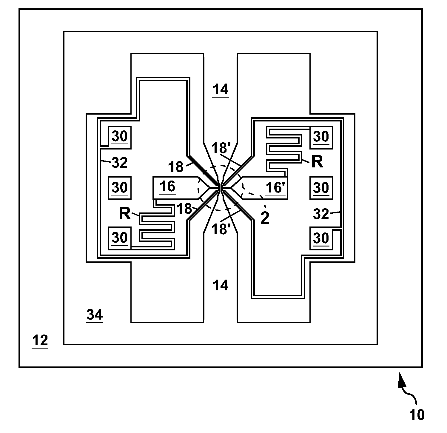
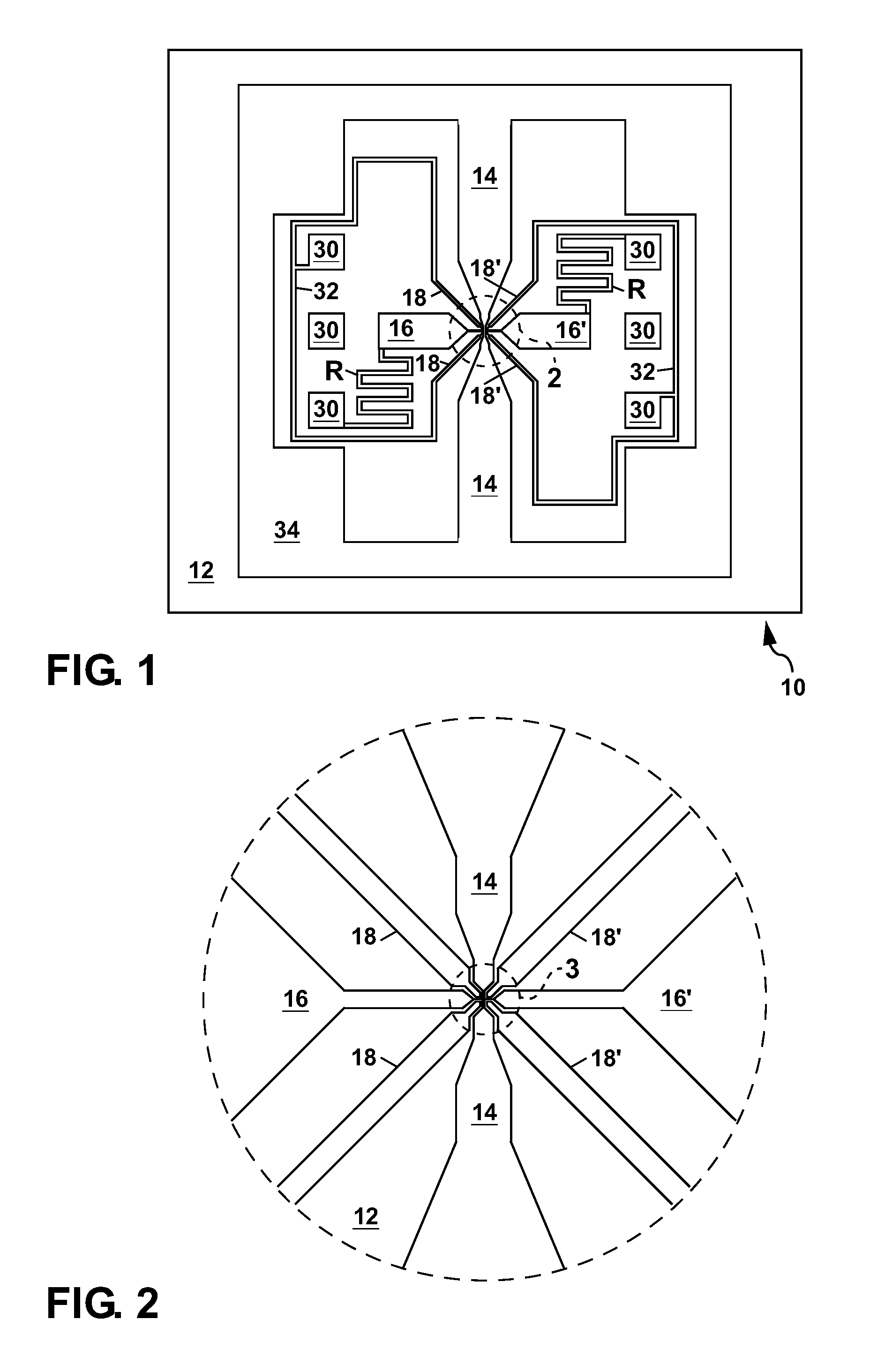
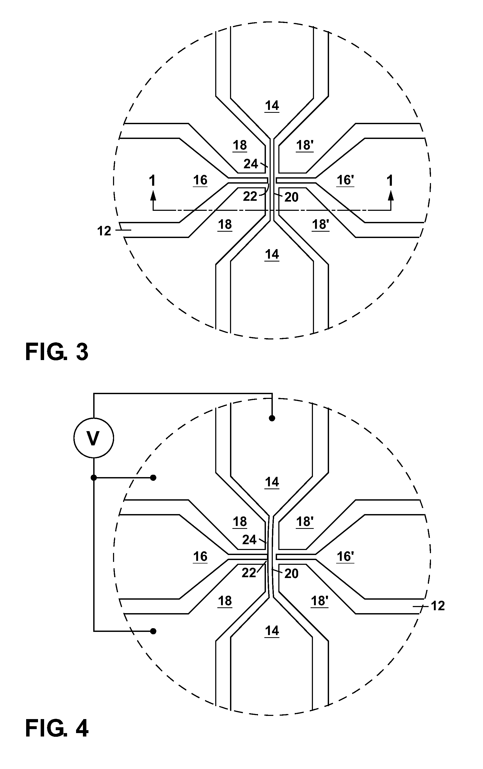
[0047]Referring to FIG. 1, there is shown a schematic plan view of an example of the NEM switching device 10 of the present invention. The NEM switching device 10, which is also referred to herein as a NEM switch or a NEM transistor, comprises a substrate 12 with a source electrode 14, two drain electrodes 16 and 16′ and two pairs of gate electrodes 18 and 18′. FIG. 2 shows an enlarged view of a portion of the device 10 of FIG. 1; and FIG. 3 shows an enlarged view of a portion of the enlarged view of FIG. 2 to better show details of the electrodes 14, 16, 16′, 18 and 18′ which have extremely small dimensions down to about 100 nanometers (nm) or less.

[0048]As can be seen from the enlarged view of FIG. 3, the source electrode 14 extends between the drain electrodes 16 and 16′ and two pairs of gate electrodes 18 and 18′ and is necked down to form an electrically-conductive beam 20, with one of the drain electrodes 16 and 16′ being located on each side of the beam 20 and extending outwa...


PUM


Abstract

A nanoelectromechanical (NEM) switch is formed on a substrate with a source electrode containing a suspended electrically-conductive beam which is anchored to the substrate at each end. This beam, which can be formed of ruthenium, bows laterally in response to a voltage applied between a pair of gate electrodes and the source electrode to form an electrical connection between the source electrode and a drain electrode located near a midpoint of the beam. Another pair of gate electrodes and another drain electrode can be located on an opposite side of the beam to allow for switching in an opposite direction. The NEM switch can be used to form digital logic circuits including NAND gates, NOR gates, programmable logic gates, and SRAM and DRAM memory cells which can be used in place of conventional CMOS circuits, or in combination therewith.

Description

GOVERNMENT RIGHTS[0001]This invention was made with Government support under Contract No. DE-AC04-94AL85000 awarded by the U.S. Department of Energy. The Government has certain rights in the invention.FIELD OF THE INVENTION[0002]The present invention relates to nanoelectromechanical (NEM) switching devices and to logic circuits formed therefrom.BACKGROUND OF THE INVENTION[0003]As CMOS transistors continue to be scaled down in size with each new generation, the sub-threshold leakage power (also referred to as the stand-by power) in these transistors becomes an increasing fraction of the total power dissipation. This has lead researchers to explore potential alternatives to CMOS technology. NEM switching devices, when used as a replacement for CMOS transistors or used in combination with CMOS transistors promise to substantially reduce or eliminate the sub-threshold leakage power which is present with CMOS transistors. NEM switching devices also promise advantages in terms of increase...

Claims


Application Information

Patent Timeline
Patent Type & Authority Patents(United States)
IPC IPC(8): H03K19/20
CPCG11C23/00H03K19/20H03K19/02G11C16/3418H01H1/0094Y10S977/724Y10S977/94
Inventor NORDQUIST, CHRISTOPHER D.CZAPLEWSKI, DAVID A.
Owner NAT TECH & ENG SOLUTIONS OF SANDIA LLC
Why Eureka
Try Eureka