Device and method for improved power distribution for a transparent electrode

a technology of led materials and transparent electrodes, which is applied in the manufacture of electrode systems, electric discharge tubes/lamps, and discharge tubes luminescnet screens, etc., can solve the problems of limited current-carrying capacity of such electrodes, limited power supply to led materials, and limited light emitted, so as to improve the power distribution of top-emitters

Active Publication Date: 2010-05-25
GLOBAL OLED TECH
View PDF9 Cites 42 Cited by
  • Summary
  • Abstract
  • Description
  • Claims
  • Application Information

AI Technical Summary

Problems solved by technology

However, the current-carrying capacity of such electrodes is limited, thereby limiting the amount of power that can be supplied to the LED materials, and hence the amount of light that can be emitted from the light-emissive layers.
Because suitable transparent conductors, for example ITO, have a limited conductivity, the current that may be passed through the organic layers 14 is limited and the uniformity of the light-emitting areas in an OLED device may be adversely affected by differences in current passed through various portions of the transparent conductor 16.
However, the formation of the auxiliary electrode 70 is problematic.
Sputtering through a shadow mask is difficult for large substrates due to thermal expansion and alignment problems of the shadow mask.
Likewise, evaporative deposition of conductive materials such as metals requires high temperatures and suffers from the same mask problems.
High temperatures may also destroy any temperature-sensitive underlying layers.
The use of photolithography to pattern an auxiliary electrode may compromise the integrity of underlying layers, particularly for organic devices.
However, these disclosures do not address the robustness of any manufacturing process required to form patterned conductors in electrical contact with a transparent electrode and may suffer from the problems cited above.
Although lower temperatures may be employed with smaller-diameter particles, the sintering time tends to be longer.
Moreover, the deposition and removal of any uncured composition may be difficult in the presence of any other environmentally sensitive materials.
Applicants have demonstrated that the process of removing unannealed material can damage underlying sensitive materials in light-emissive areas.
Commercial, patterned deposition methods, such as inkjet devices, may not provide the resolution necessary to avoid occluding light emission from a top-emitter LED device.
In practice in any process it is difficult to avoid some direct reaction of the different precursors leading to a small amount of chemical vapor deposition reaction.
While CVD and / or ALD processes may be useful for encapsulating environmentally sensitive devices, such layers as described in the prior art tend to be insulating layers and therefore are not useful for improving the conductivity of transparent electrodes.

Method used


Image

  • Device and method for improved power distribution for a transparent electrode
  • Device and method for improved power distribution for a transparent electrode
  • Device and method for improved power distribution for a transparent electrode

Examples


Embodiment Construction

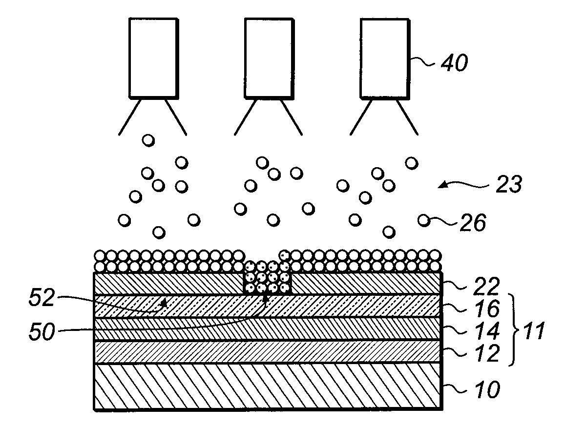
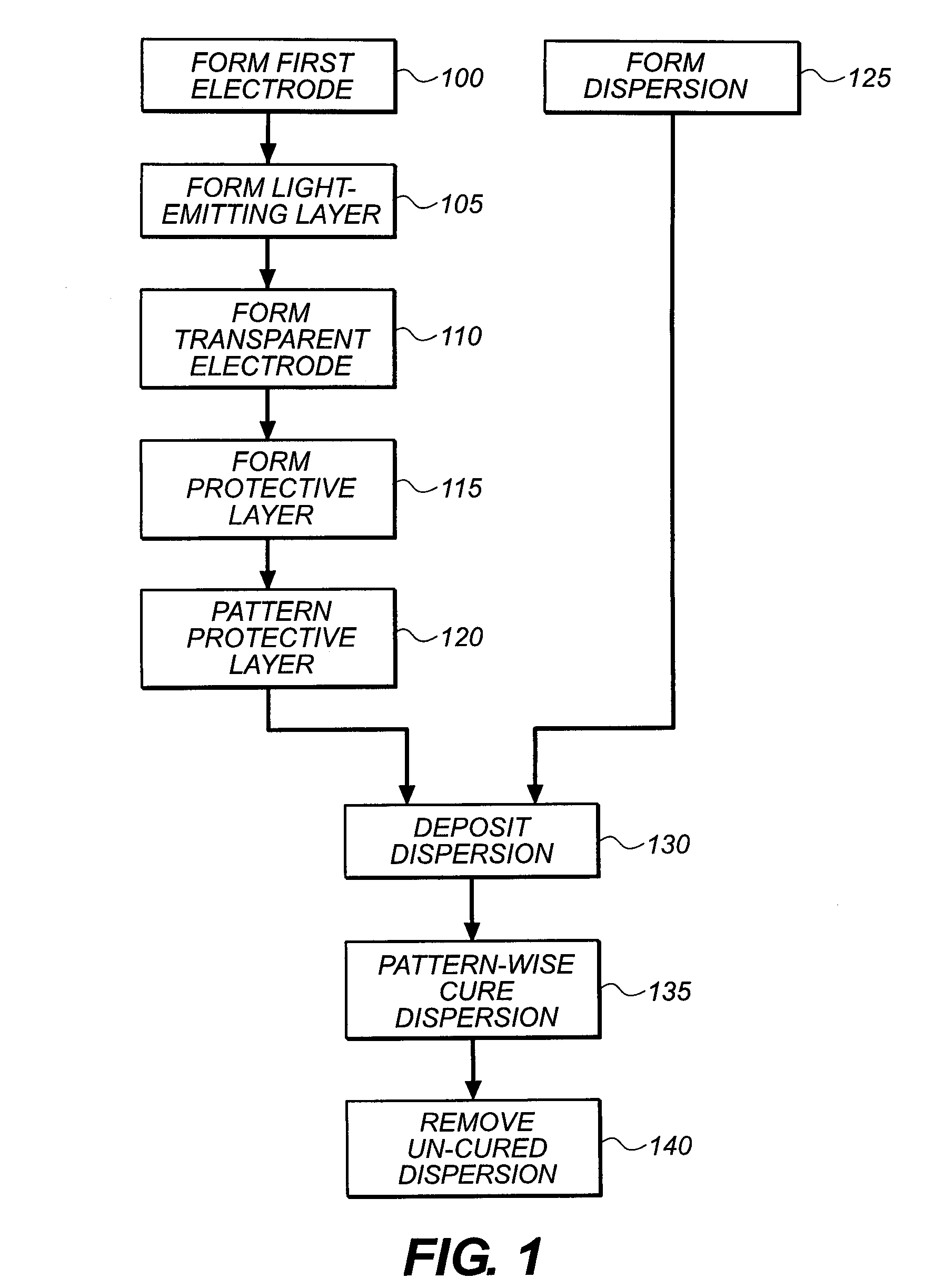
[0036]Referring to FIG. 1, a method for improving power distribution of a transparent electrode in a light-emitting diode (LED) device, comprises the steps of forming an LED over a substrate, the LED including a first electrode, a transparent electrode, and one or more light-emissive layers formed there-between. The LED is made by forming 100 a first electrode over a substrate, forming 105 one or more light-emissive layers over the first electrode, and then forming 110 a transparent electrode over the light-emissive layers to make a light-emitting diode (LED). A patterned protective layer is formed on the transparent electrode, the patterned protective layer having open areas wherein the protective layer is not present and covered areas wherein the protective layer is present. For example, an unpatterned protective layer may be first formed 115 by a chemical vapor deposition process over the transparent electrode and then patterned 120 using laser ablation. A solution, for example, ...


PUM

PropertyMeasurementUnit
diametersaaaaaaaaaa
humidityaaaaaaaaaa
diameteraaaaaaaaaa

Abstract

A method for improving power distribution of a transparent electrode that includes forming an LED over a substrate; the LED including a first electrode, a transparent electrode, and one or more light-emissive layers formed there-between. A patterned protective layer is formed on the transparent electrode; the patterned protective layer having open areas wherein the protective layer is not present, and covered areas wherein the protective layer is present. A solution having curable conductive precursor components is deposited over the open areas onto the transparent electrode. The precursor components of the solution are pattern-wise cured to form patterned electrically conductive areas on the transparent electrode in the open areas, and any uncured precursor components of the solution are removed.

Description

FIELD OF THE INVENTION[0001]The present invention relates to top-emitting light-emitting diode (LED) devices, and more particularly, to a method for improving power distribution in a transparent electrode.BACKGROUND OF THE INVENTION[0002]Light-emitting diodes (LEDs) are a promising technology for flat-panel displays and area illumination lamps and backlights. Applications of LED devices include active-matrix image displays, passive-matrix image displays, and area-lighting devices such as, for example, selective desktop lighting. Irrespective of the particular LED device configuration tailored to these broad fields of applications, all LEDs function on the same general principles. An electroluminescent (EL) medium structure is sandwiched between two electrodes. At least one of the electrodes is at least partially light transmissive. These electrodes are commonly referred to as an anode and a cathode in analogy to the terminals of a conventional diode. When an electrical potential is ...

Claims


Application Information

Patent Timeline
Patent Type & Authority Patents(United States)
IPC IPC(8): H01J9/20H01J1/54
CPCH01L51/5203H01L51/5237H01L51/5234H10K50/805H10K50/828H10K50/841
Inventor COK, RONALD S.
Owner GLOBAL OLED TECH
Why Eureka
Try Eureka