Image capturing apparatus

a technology of image capturing and image, which is applied in the direction of radio frequency control devices, instruments, television systems, etc., can solve the problems of unwanted charges, storage parts, and difficulty in performing simultaneous electronic shutter operation for all pixels, and achieve the effect of removing the influence of leakag

Active Publication Date: 2010-06-08
CANON KK
View PDF9 Cites 112 Cited by
  • Summary
  • Abstract
  • Description
  • Claims
  • Application Information

AI Technical Summary

Benefits of technology

[0007]An object of the present invention is to eliminate the influences of the leakage etc. of charges from a photodiode to a storage part during the electronic shutter operation.

Problems solved by technology

With this sensor, however, it is difficult to perform a simultaneous electronic shutter operation for all pixels as employed in interline type CCD image sensors, due to such reasons as the usage voltage being limited, or the number of elements constituting one pixel being large.
Therefore, while the charges are being held in the storage part 1e, i.e., during a time period from when the charges of the photodiode PD are transferred to the storage part 1e to when the charges are outputted via the amplifier JFET, unwanted charges may leak from the photodiode PD, or the storage part 1e may be directly exposed to light to generate unwanted charges.
Also, even when the electronic shutter operation is not needed, the charges must be transferred via the first transfer part 1a, storage part 1e and second transfer part 1b, thus making the operation complex.

Method used


Image

  • Image capturing apparatus
  • Image capturing apparatus
  • Image capturing apparatus

Examples


first embodiment

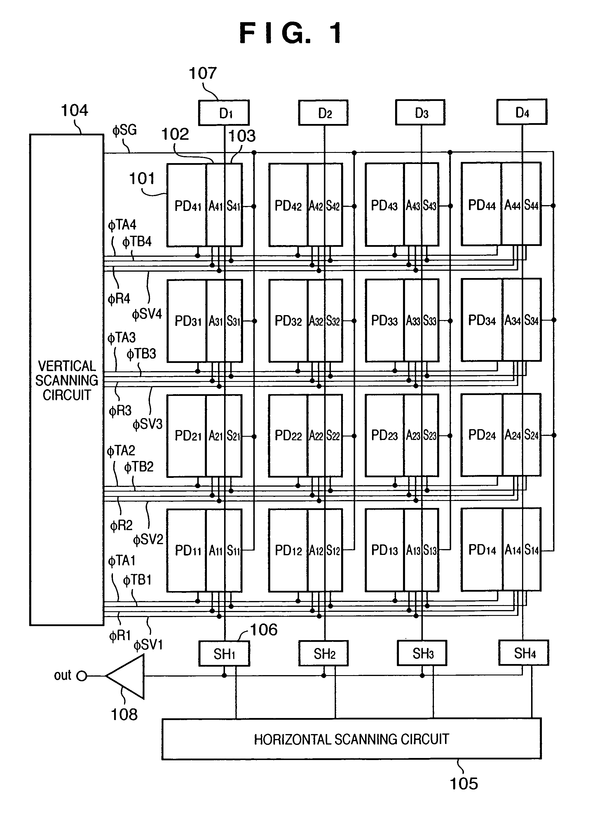
[0024]FIG. 1 is a diagram showing a configuration of a CMOS image sensor according to a first embodiment of the present invention.

[0025]Referring to FIG. 1, reference numeral 101 denotes a photodiode which generates and accumulates a signal charge according to incident light; 102 denotes an output part; 103 denotes a storage part which temporarily holds the charge; 104 denotes a vertical scanning circuit for performing a selection of row direction to scan all rows; 105 denotes a horizontal scanning circuit for performing a selection of column direction to scan columns; 106 denotes a sample hold circuit which temporarily stores an image signal of a row selected by the vertical scanning circuit to allow the horizontal scanning circuit 105 to scan the image signal; 107 denotes a constant electric current source for driving the output part 102; 108 denotes an output amplifier for outputting to the outside of the image sensor the image signal stored in the sample hold circuit 106 and sel...

second embodiment

[0047]Next, a second embodiment of the present invention will be described.

[0048]FIG. 4 is a diagram illustrating two pixels constituting an image sensor according to a second embodiment. In FIG. 4, the same reference numerals are applied to parts corresponding to FIG. 2, and an explanation thereof is omitted.

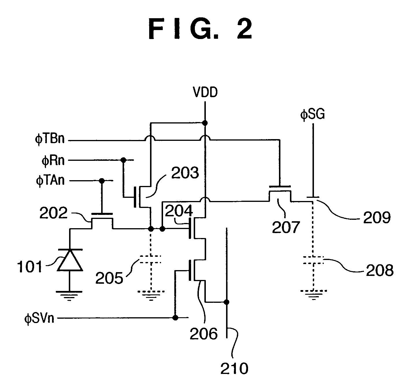
[0049]Referring to FIG. 4, reference numerals 110a and 101b denote photodiodes. Reference numeral 202a denotes a transfer gate for transferring charges from the photodiode 110a to a storage capacitor 205 of an output part 102, the transfer gate being controlled by transfer pulse φTAn. Reference numeral 202b denotes a transfer gate for transferring charges from the photodiode 101b to the storage capacitor 205 of the output part 102, the transfer gate being controlled by transfer pulse φTAn+1. Reference numeral 207a denotes a transfer gate for transferring signal charges of the storage capacitor 205 of the output part 102 to a storage capacitor 208a of a storage part 103, the tra...

third embodiment

[0072]Next, a third embodiment of the present invention will be described.

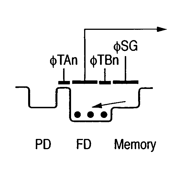
[0073]FIGS. 6A to 6F are diagrams showing drive timing and potential of an image sensor according to the third embodiment. An electronic shutter operation of the third embodiment will be described with reference to FIGS. 2 and 6A to 6F. Referring to FIGS. 6A to 6F, reference character PD denotes potential of the photodiode 101; reference character FD denotes potential of the storage capacitor 205 of the output part 102; reference character Memory denotes potential of the storage capacitor 208 of the storage part 103.

[0074]Firstly the electronic shutter operation, i.e., the operation from the initiation of accumulation of signal charges by the photodiode 101 to the transfer of the signal charges to the storage capacitor 208 of the storage part 103 will be described.

[0075]At time t0, transfer pulse φTAn is turned off to initiate the generation and accumulation of signal charges by the photodiode 101. FIG. 6B is ...


PUM


Abstract

An object of the present invention is to eliminate the influences of the leakage etc. of charges from a photodiode to a storage part during the electronic shutter operation. To achieve this object, the present invention includes: a photodiode which generates and accumulates a signal charge according to the amount of light from an object; an amplification part which amplifies a signal charge outputted from the photodiode and outputs the amplified signal to the outside; a storage part which temporarily stores the signal charge; and a transfer device which transfers the signal outputted from the photo-electric conversion device to the storage part via the amplification part.

Description

FIELD OF THE INVENTION[0001]The present invention relates to an exposure time control technique based on an electronic shutter operation using a solid state image sensor.BACKGROUND OF THE INVENTION[0002]As an XY address type image sensor, there has hitherto be known the CMOS image sensor disclosed in IEEE TRANSACTIONS ON ELECTRON DEVICE VOL41, PP452-453, 1994, and so on. This image sensor has many advantages, such as high S / N ratio, low power consumption and on-chip peripheral circuitry. With this sensor, however, it is difficult to perform a simultaneous electronic shutter operation for all pixels as employed in interline type CCD image sensors, due to such reasons as the usage voltage being limited, or the number of elements constituting one pixel being large.[0003]To overcome this drawback, there has been proposed, for example, a configuration of the image sensor described in Japanese Patent Laid-Open No. 11-177076. In this conventional CMOS image sensor, in order to implement a ...

Claims


Application Information

Patent Timeline
Patent Type & Authority Patents(United States)
IPC IPC(8): H04N3/14H01L27/00H04N5/335H01L27/146H04N5/353H04N5/359H04N5/374H04N5/3745H04N5/376
CPCH04N5/2353H04N5/3532H04N5/37457H04N5/3741H04N5/37452H04N5/359H04N23/73H04N25/531H04N25/62H04N25/766H04N25/778H04N25/771
Inventor TAKEDA, NOBUHIRO
Owner CANON KK
Why Eureka
Try Eureka