Broadband active balun
a balun and broadband technology, applied in the direction of amplifiers, amplifiers with semiconductor devices only, amplifiers, etc., can solve the problems of sacrificing the bandwidth's lower-end frequency, increasing costs, and affecting the stability of the band, so as to achieve the effect of improving stability
- Summary
- Abstract
- Description
- Claims
- Application Information
AI Technical Summary
Benefits of technology
Problems solved by technology
Method used
Image
Examples
example 1
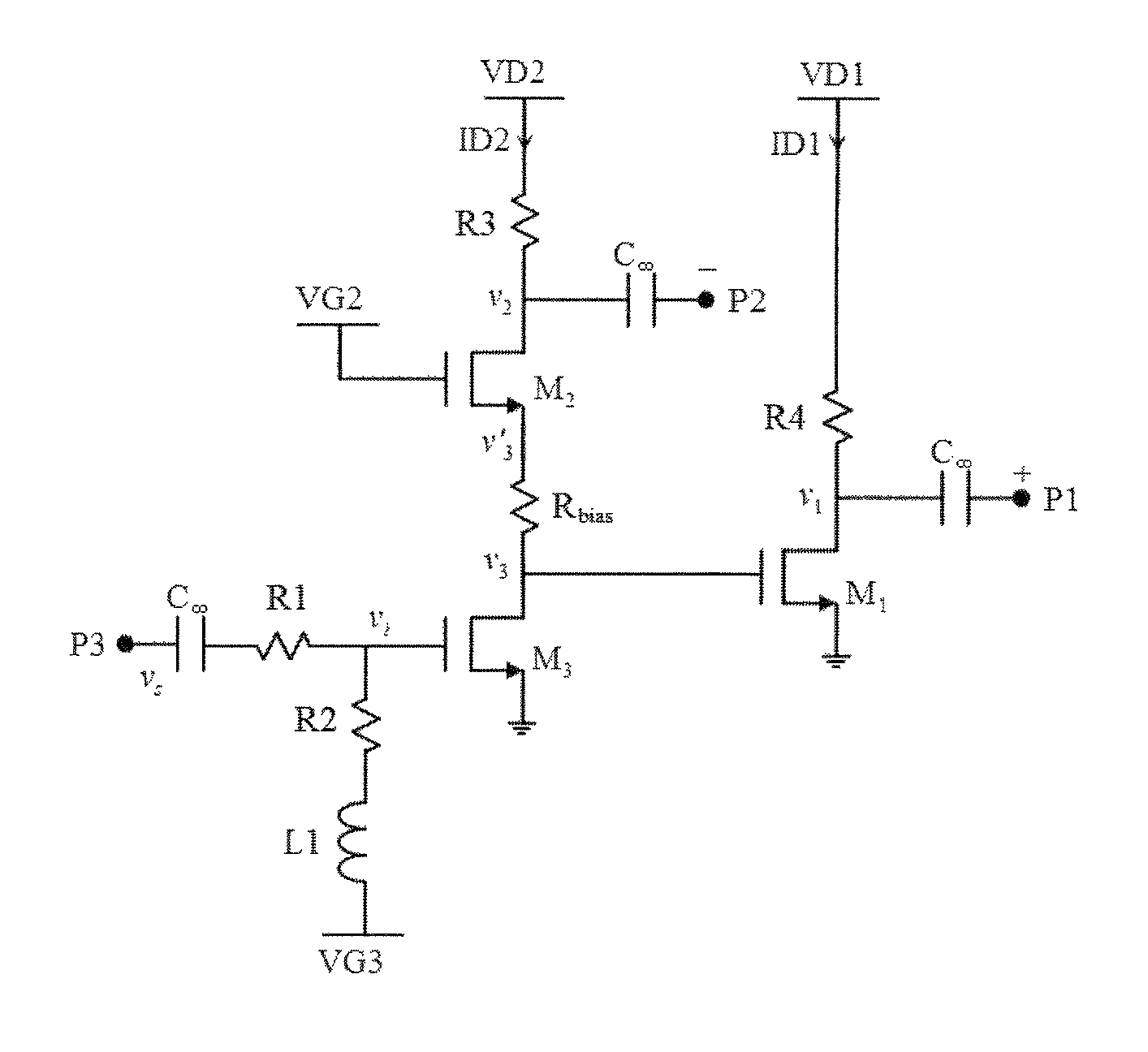
[0046]In a specific example implementation, a source-type active balun is provided. The active balun configuration uses a cascode and cascade pair with the shared input transistor. The schematic for the C3-balun is shown in FIG. 5, where the transconductance for each transistor is annotated in parenthesis. The broadband input matching can be further enhanced by dividing the input's 50 Ω resistance into 22.6 Ω and 27.0 Ω, where the remaining 0.3 Ω is from the parasitic resistance of the 0.2 nH inductor. The dividing of the 50 Ω resistance can reduce the input signal, but requires the increase of the size of M3. An Rbias of 4.7 Ω is introduced to enable additional design freedom, so that bias point of M2's source, ν′3, can be chosen to be different from that of M3's drain and M1's gate, ν3. The bias-points are optimally chosen for the circuit to operate up to 5 dBm of the input power, while maintaining all transistors to operate in the saturation-mode and remain safe from gate-drain a...
example 2
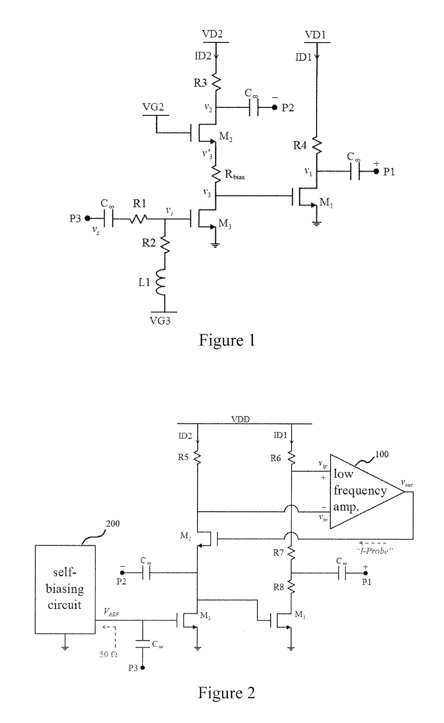
[0061]In a further example a low-pass bias-feedback mechanism can be incorporated in the C3-balun. As shown in FIG. 17, in a specific implementation, the drain currents of ID1 and ID2 are matched to 17.12 mA, and the lower-end terminals of the two 62.9 Ω resistors are connected to νip and νin. The low-pass bias-feedback network can control the matching of s13 and s23. The values of the matched magnitudes of s13 and s23 can then be maintained at −3 dB each by controlling the ID1 and ID2 bias currents using the self biasing circuit.
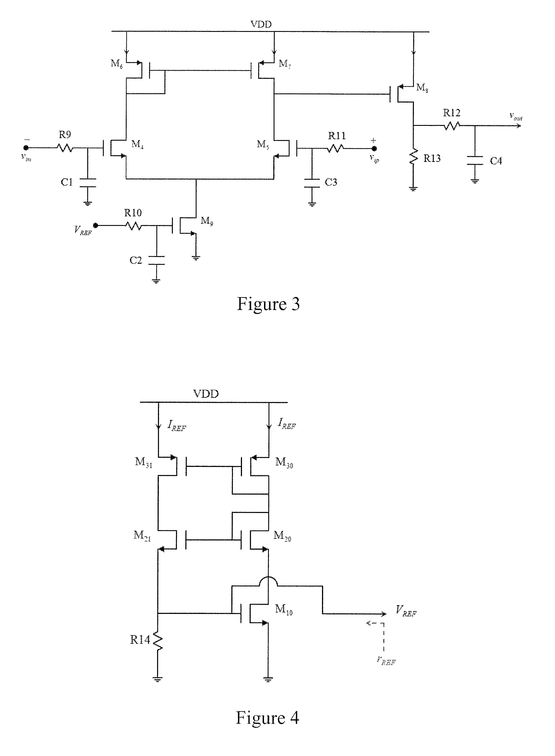
[0062]The circuit diagram for the low-frequency amplifier is shown in FIG. 18. The matching of the drain currents enables the matching of the transconductances of M3 and M1, which results in the matching of s13 and s23 magnitudes.
[0063]The low-pass bias-feedback network only controls the matching of s13 and s23 and not their values, which need to be maintained at −3 dB each. Since the values of the matched s13 and s23 depend on the matched bias currents of ...
PUM
 Abstract
Description
Claims
Application Information


