Wavelength converting devices
a conversion device and wavelength technology, applied in the direction of instruments, optical waveguide light guides, light demodulation, etc., can solve the problems of difficult to oscillate converted light of a high output power of, for example, 1 w or more, and the limit of the resistance against optical damage, etc., to achieve the effect of limiting the conversion efficiency of fundamental light to harmonic wave, and reducing the output power
- Summary
- Abstract
- Description
- Claims
- Application Information
AI Technical Summary
Benefits of technology
Problems solved by technology
Method used
Image
Examples
example 1
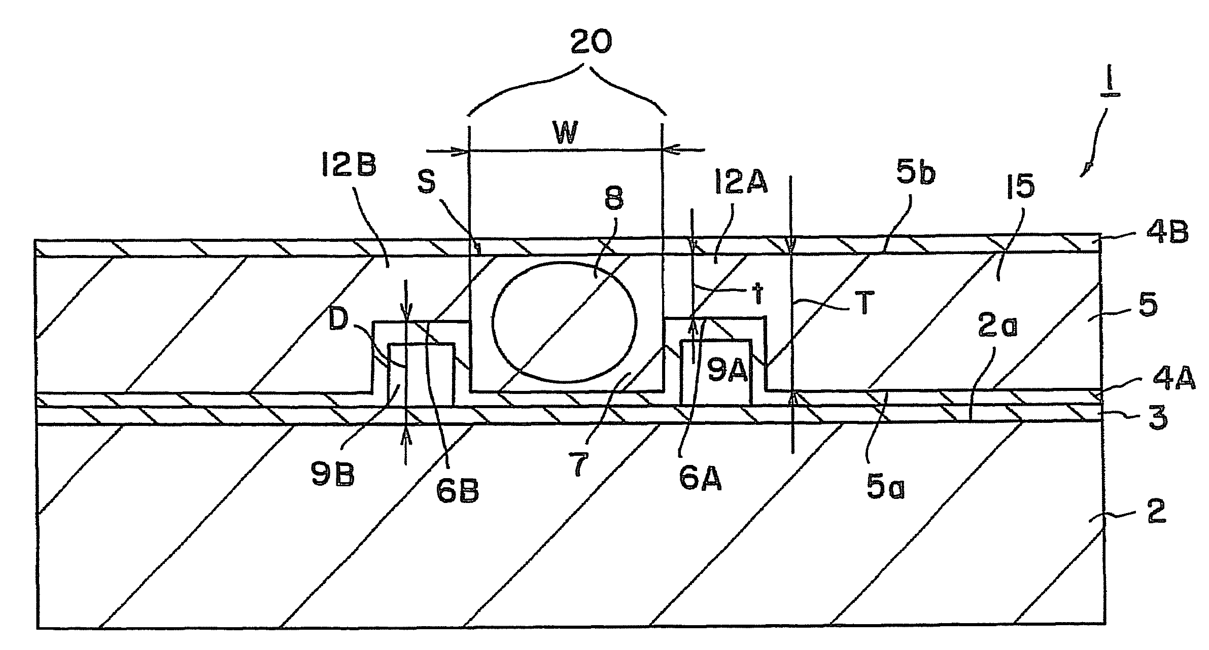
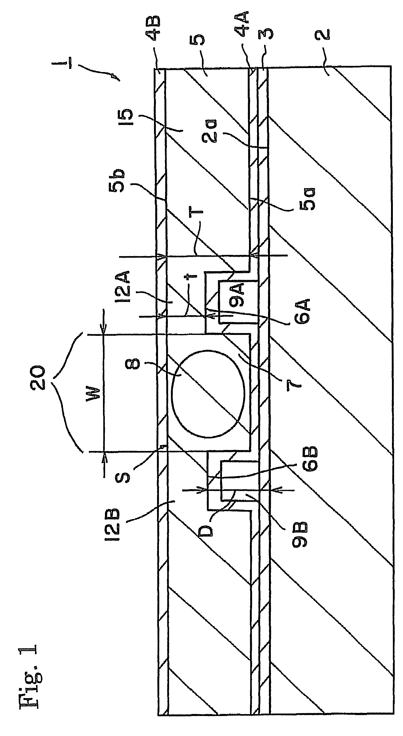
[0060]The device 1 described referring to FIG. 1 was produced.
[0061]Specifically, periodic polarization domain inversion structure having a period of 6.54 μm was produced in a Z-cut substrate having a thickness of 500 μm and made of MgO-doped lithium niobate. SiO2 film having a thickness of 0.5 μm was formed thereon by sputtering. Further, Mo film of a thickness of 0.5 μg / m was formed by sputtering and then patterned to produce an etching mask. Wet etching was then performed in a fluoric acid solution heated at 60° C. to form the grooves 6A and 6B. The depth “D” of the groove was 20 μm and the distance between the grooves was 50 μm.
[0062]An adhesive was applied on the substrate 2 having a thickness of 1 mm and made of non-doped lithium niobate. The substrate 2 was then adhered to the above substrate 5 of MgO-doped lithium niobate. The surface 5b of the substrate 5 of MgO-doped lithium niobate was removed by grinding and polishing to a thickness of 50 μm. SiO2 film 4B having a thickn...
example 2
[0064]The device 1 described referring to FIG. 1 was produced.
[0065]Periodic polarization domain inversion structure having a period of 6.54 μm was produced in a Z-cut substrate having a thickness of 500 μm and made of MgO-doped lithium niobate. SiO2 film having a thickness of 0.5 μm was formed by sputtering. Further, Mo film of a thickness of 0.5 μm was formed by sputtering and then patterned to produce an etching mask. Wet etching was then performed in a fluoric acid solution heated at 60° C. to form the grooves 6A and 6B. The depth “D” of the groove was 5 μm and the distance between the grooves was 100 μm.
[0066]An adhesive was applied on the substrate 2 having a thickness of 1 mm and made of non-doped lithium niobate. The substrate 2 was then adhered to the above substrate 5 of MgO-doped lithium niobate. The surface 5b of the substrate 5 of MgO-doped lithium niobate was removed by grinding and polishing to a thickness of 10 μm. Ta2O5 film 4B having a thickness of 0.5 μm was forme...
PUM
| Property | Measurement | Unit |
|---|---|---|
| cross sectional area | aaaaa | aaaaa |
| cross sectional area | aaaaa | aaaaa |
| output power | aaaaa | aaaaa |
Abstract
Description
Claims
Application Information


