Split chip

a technology of split chips and chips, applied in the field of rfid, can solve the problems of inability to retain data, no manner in which information or data on the memory section can be radiated, etc., and achieve the effects of increasing the range and selectivity reducing the cost of the rfid system, and increasing the absorption rate of electromagnetic signals

Inactive Publication Date: 2010-06-22
RODGERS JAMES NEIL
View PDF5 Cites 3 Cited by
  • Summary
  • Abstract
  • Description
  • Claims
  • Application Information

AI Technical Summary

Benefits of technology

[0016]This invention also refers to Rodgers application Ser. No. 11 / 683,056 titled, “RFID silicon antenna,” which is incorporated herein by reference. The RFID silicon antenna is a system of producing an RFID antenna using the silicon in an integrated circuit as the resonant antenna material for the purpose of reducing the cost of an RFID system and for the purpose of increasing the range and selectivity of the RFID system. According to the RFID silicon antenna invention the base silicon sheets which make up the primary building material of the silicon chip (integrated circuit) is subjected to a laser ablation process. This creates three dimensional nano structures on the surface of the silicon thereby raising its absorption rate of electromagnetic signals. On the reverse side of the same silicon sheet a directional antenna is etched using standard photographic reduction techniques and standard semi conductor industry manufacturing methods. The two sides of the silicon are connected through doping aluminum or copper impurities into these same base silicon sheets causing conductivity within the sheet of silicon.

Problems solved by technology

The half of the silicon circuit which contains the antenna and active transistor half has no memory transistors and therefore cannot retain data.
There is no manner in which the information or data on the memory section can be radiated from this half of the bifurcated circuit.

Method used


Image

  • Split chip
  • Split chip
  • Split chip

Examples


embodiment

PREFERRED EMBODIMENT

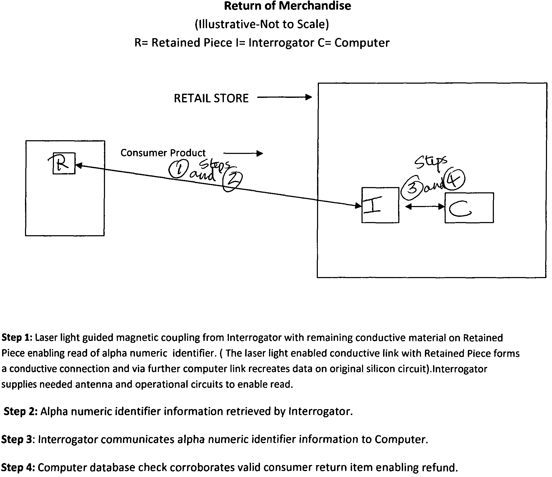
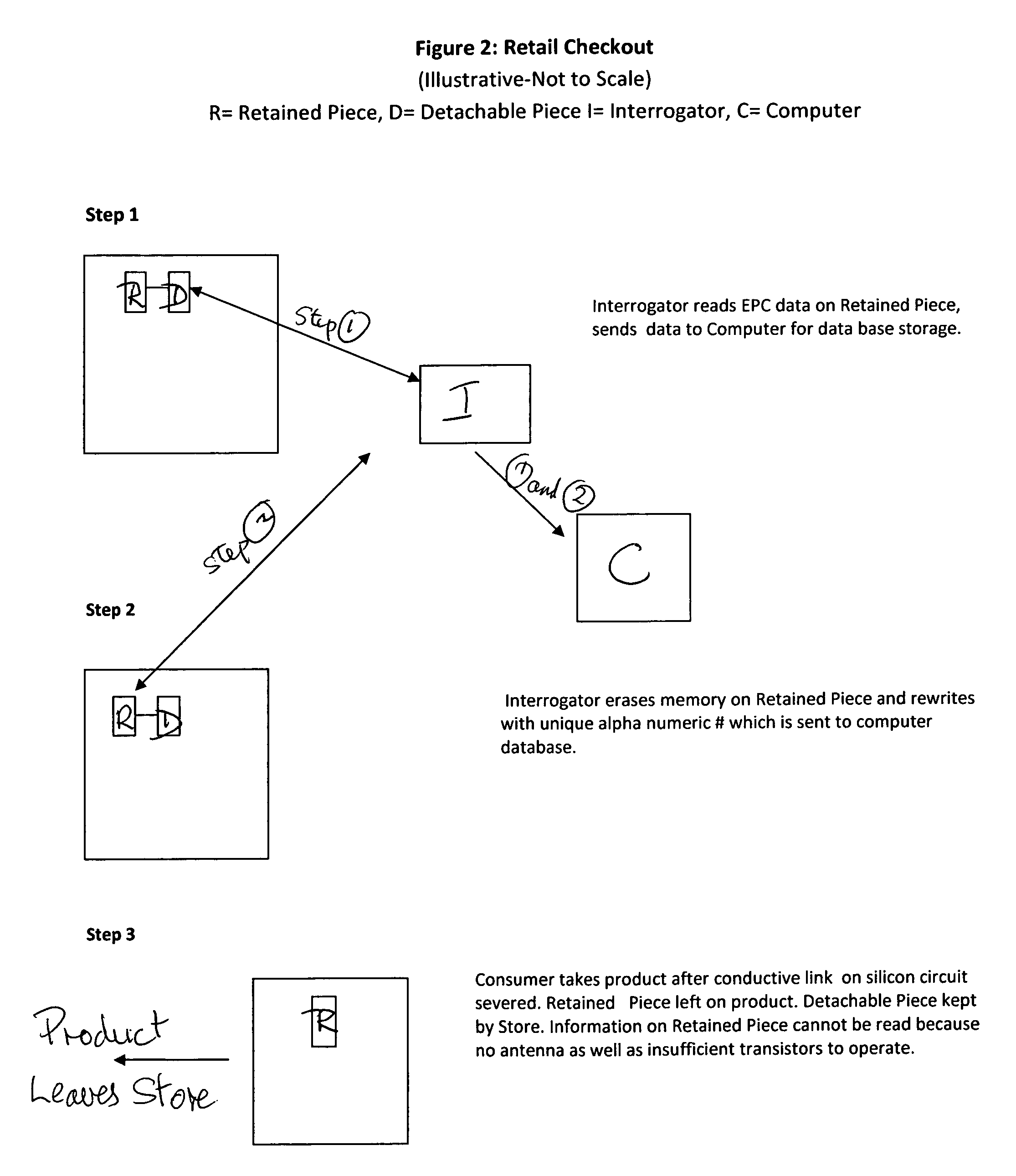
[0048]This present invention, in a preferred embodiment, contemplates a Split Chip method and system as part of the Clip Chip method and system. Accordingly, when a consumer severs the RFID transponders after purchase the RFID transponder is moribund. In the circumstance of a refund or return of consumer item, the circuitry can be reconnected as per the Clip Chip methodology and as outlined above.

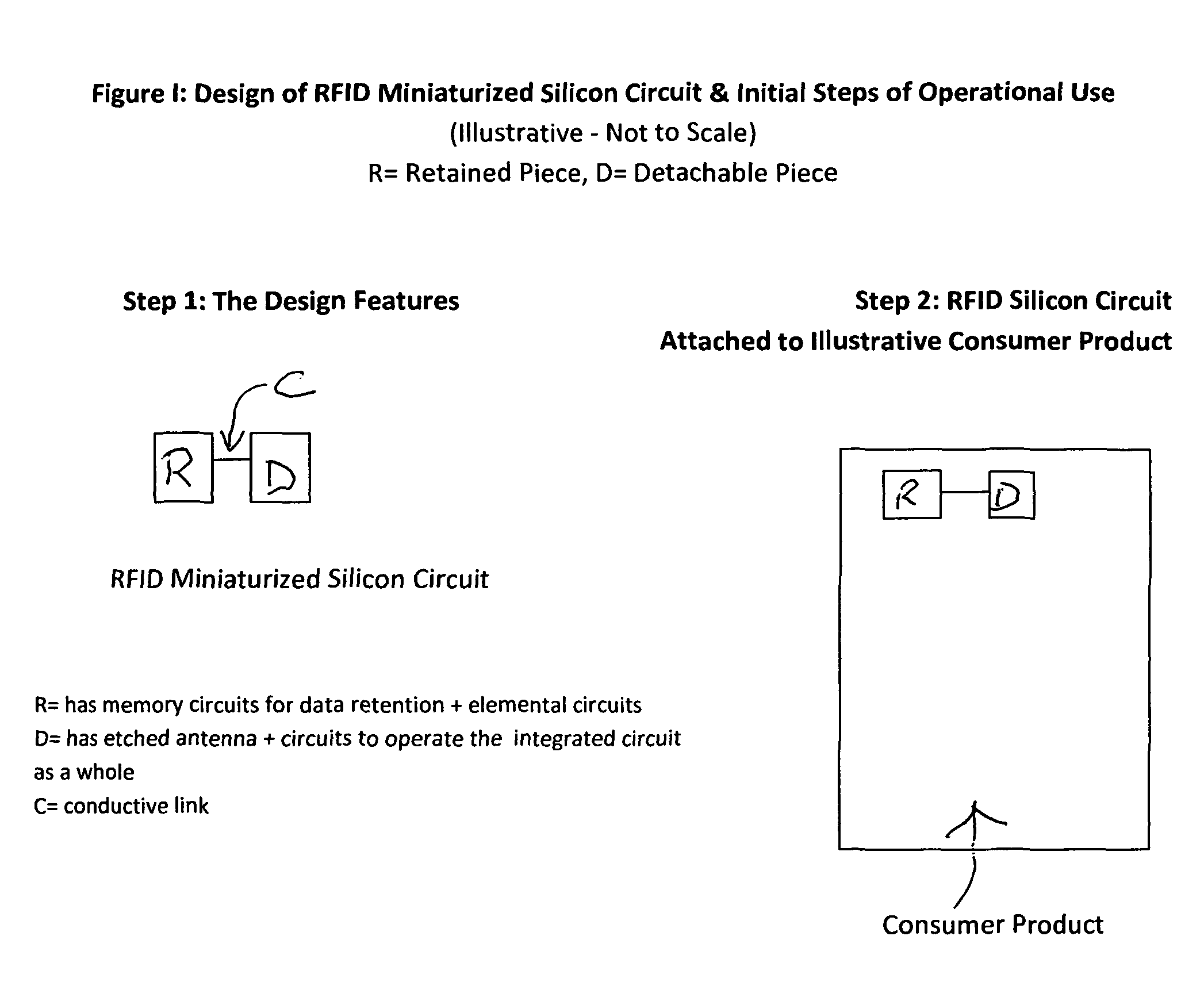
[0049]The useful, non-obvious and novel steps of this Invention are the design of an integrated silicon circuit as two separate pieces connected by a fine piece of conductive material such as conductive ink. Each piece is dependent upon the other in order to function. The two pieces, when separated, provide the benefit and function to consumers of complete consumer privacy as the RFID transponders cannot be skimmed of data once separated. In the circumstance of a consumer requirement to reactivate the RFID tag, such as a returned consumer item to a retail outlet, a retur...


PUM


Abstract

The Invention, titled the “Split Chip” by the Inventor, contemplates an RFID enabled consumer oriented tracking system which protects consumer privacy by splitting a miniaturized silicon RFID transponder circuit into a retained piece and a detached piece. The two pieces are electrically connected by a fine piece of conductive material. Each piece is dependent upon the other in order to disgorge data. The electrical connection between the two pieces can be severed by the consumer by tearing the fine piece of conductive material at a designated spot on the substrate making the Split Chip moribund. Upon a return or refund of the consumer item the original data can be recovered through a laser guidance system which connects the retained piece and its alpha numeric identifier to a back end host computer administration network.

Description

CROSS REFERENCE TO RELATED APPLICATIONS[0001]PG 20080252454, Clip Chip, Rodgers, herewith incorporated by reference[0002]PG 20080217560, RFID Silicon Antenna, Rodgers, herewith incorporated by referenceSTATEMENT REGARDING FEDERALLY SPONSORED RESEARCH OR DEVELOPMENT[0003]Not ApplicableTHE NAMES OF PARTIES TO A JOINT RESEARCH AGREEMENT[0004]Not ApplicableINCORPORATION-BY REFERENCE OF MATERIAL SUBMITTED ON A COMPACT DISC[0005]Not ApplicableBACKGROUND OF THE INVENTION[0006]1. Field of the Invention[0007]The field of the invention is Radio Frequency Identification (RFID) and in particular an RFID enabled consumer oriented system which protects consumer privacy.[0008]2. Background[0009]Radio Frequency Identification (hereinafter “RFID”), is a technology powered by small, wireless devices known as tags or transponders which can automatically track physical objects, animals and people when air interfacing with RFID readers, also known as interrogators. RFID can be seen as a means to explici...

Claims


Application Information

Patent Timeline
Patent Type & Authority Patents(United States)
IPC IPC(8): G08B13/14
CPCG06K19/07345
Inventor RODGERS, JAMES NEIL
Owner RODGERS JAMES NEIL
Why Eureka
Try Eureka