Methods and systems stackable circuit boards

a stackable circuit board and stackable technology, applied in the field of stackable circuit boards, can solve problems such as ringing in high-speed transmission lines, and achieve the effects of reducing ringing, reducing stub length, and improving signal transmission

Inactive Publication Date: 2010-07-06
MICROSYS
View PDF6 Cites 15 Cited by
  • Summary
  • Abstract
  • Description
  • Claims
  • Application Information

AI Technical Summary

Benefits of technology

[0006]Some embodiments may use connections that offset from the bottom connector of a printed circuit board to the top connector of the same board. Offset connections allow an individual connection to be established between the processor or other type of board and each board located above or below it. In various embodiments, the first connection may be used by the first board in a stack, e.g., the first board above the processor board. The remaining connections may be shifted over in position to replace the connection used by the first board in the stack. This may continue until, for example, all a

Problems solved by technology

Stubs may cause ringing in h

Method used


Image

  • Methods and systems stackable circuit boards
  • Methods and systems stackable circuit boards
  • Methods and systems stackable circuit boards

Examples


Embodiment Construction

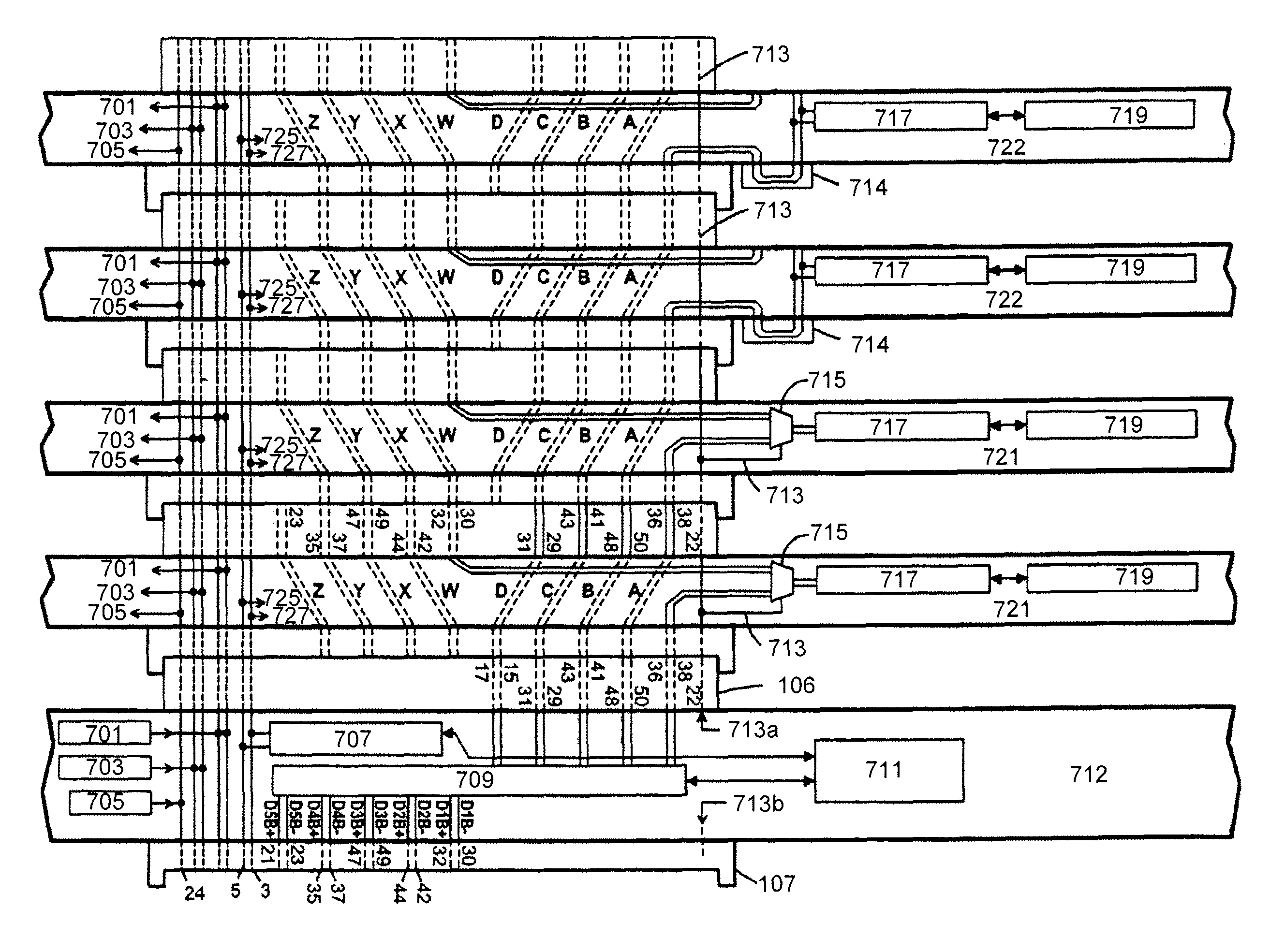
[0036]The present invention is directed toward methods and systems for providing a stackable connector system comprising a multiplexer or other switching device configured to select a signal based on a location of a first circuit board above or below a second circuit board. In some embodiments, a sense line may be coupled to a location signal and configured to indicate if the first circuit board is above or below the second circuit board. Additionally, a first connector, including a first conductor element, and a second connector, including a second conductor element, may be located on the first circuit board. An electrical connection element on the first circuit board may connect the first conductor element to the second conductor element, wherein the location of the first conductor element in the first connector may be offset relative to the location of the second conductor element in the second connector.

[0037]Before describing the invention in detail, it is useful to describe an...


PUM


Abstract

The present invention is directed toward methods and systems for providing a stackable connector system comprising a switching device configured to select a signal based on a location of a first circuit board above or below a second circuit board. A sense line may be coupled to a location signal and configured to indicate if the first circuit board is above or below the second circuit board. Additionally, a first connector, including a first conductor element, may be located on the first circuit board and a second connector, including a second conductor element, may be located on the first circuit board. An electrical connection element on the first circuit board mat connect the first conductor element to the second conductor element, wherein the location of the first conductor element in the first connector is offset relative to the location of the second conductor element in the second connector.

Description

RELATED APPLICATION INFORMATION[0001]This application claims priority to provisional application 60 / 898,663 filed Jan. 30, 2007 and provisional application 60 / 899,222 filed Feb. 1, 2007, each of which is incorporated herein by reference.FIELD OF THE INVENTION[0002]The present invention relates generally to circuit boards, and more particularly, some embodiments relate to methods and systems for stackable circuit boards.BACKGROUND OF THE INVENTION[0003]Embedded systems are used in a wide variety of applications from simple control applications to complex real-time systems. Such a system commonly comprises of a processor board and several peripheral boards that are stacked above the processor board, with a parallel bus provided from the processor board to the peripheral boards through a stack of interconnecting connectors on the boards. The processor board may be called a single-board computer or SBC for short. Each peripheral board can provide a wide variety of functions, ranging fro...

Claims


Application Information

Patent Timeline
IPC IPC(8): H01R12/00
CPCG06F13/409H04Q1/08H05K1/144H05K7/023H04Q1/03H05K1/0268H05K2201/042H05K2201/10053H05K2201/10189H01R12/716
Inventor WOOLEY, SUSANKUBOTA, GLENN S.MAIN, DALE
Owner MICROSYS
Why Eureka
Try Eureka