Semiconductor module and method of manufacturing the same

a technology of semiconductors and modules, applied in the direction of solid-state device testing/measurement, semiconductor/solid-state device testing/measurement, basic electric elements, etc., can solve the problems of snubber circuits, insufficient reduction of ringing, damage to semiconductor modules, etc., and achieve high switching speed and reduce ringing

Active Publication Date: 2021-05-13
FUJI ELECTRIC CO LTD
View PDF0 Cites 5 Cited by
  • Summary
  • Abstract
  • Description
  • Claims
  • Application Information

AI Technical Summary

Benefits of technology

[0009]In view of the foregoing problem, the present invention provides a semiconductor module and a method of manufacturing the semiconductor module capable of reducing ringing caused during a switching operation of a switching element, regardless of the use of a wide bandgap semiconductor particularly having a high switching speed.

Problems solved by technology

If a peak value of a voltage upon ringing exceeds a rated voltage of the semiconductor module, the semiconductor module may be damaged.
The use of such a snubber circuit still has a problem of an insufficient reduction in the ringing particularly when a frequency is high.

Method used


Image

  • Semiconductor module and method of manufacturing the same
  • Semiconductor module and method of manufacturing the same
  • Semiconductor module and method of manufacturing the same

Examples


first embodiment

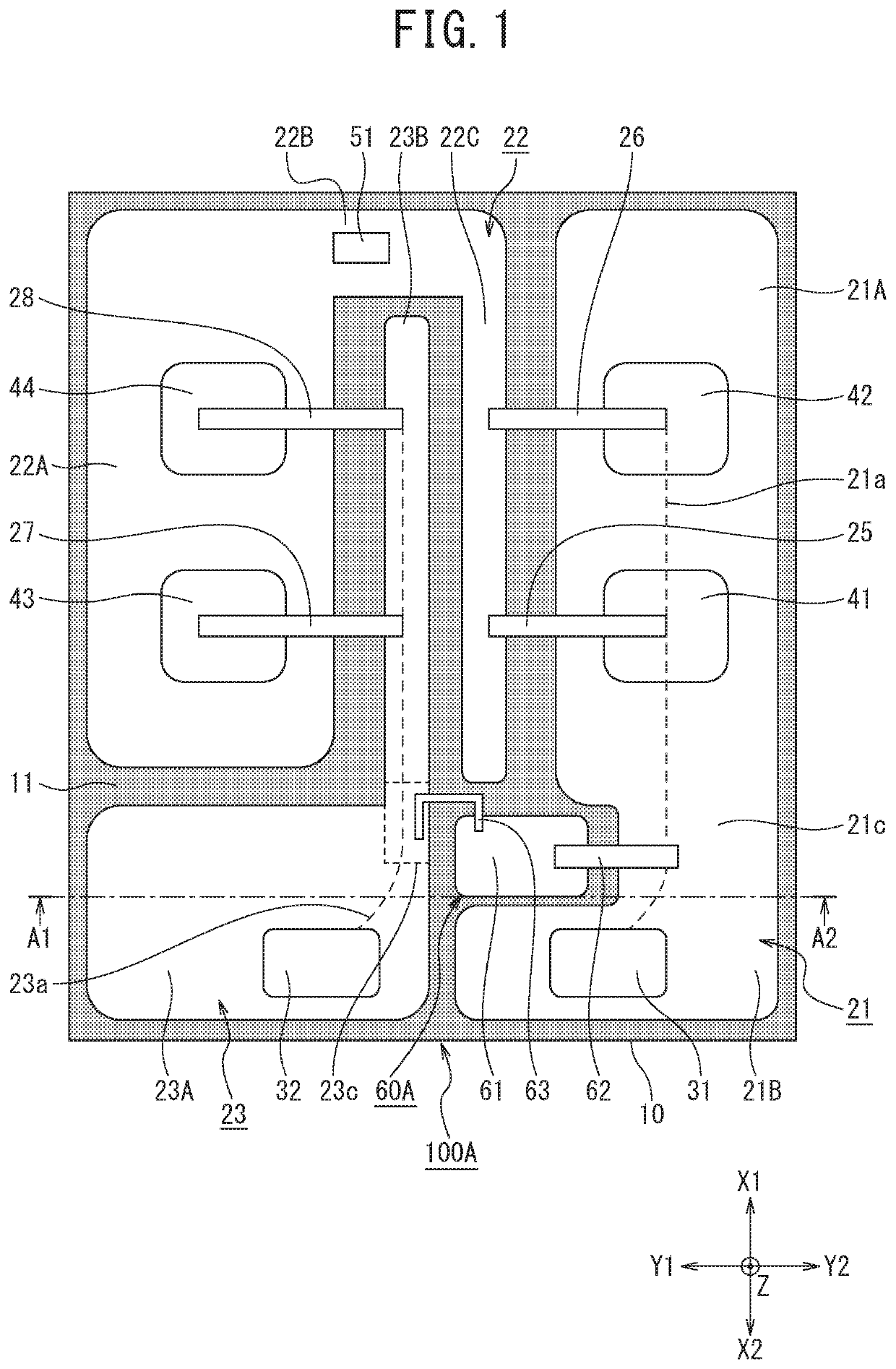
[0023](Configuration of Semiconductor Module 100A)

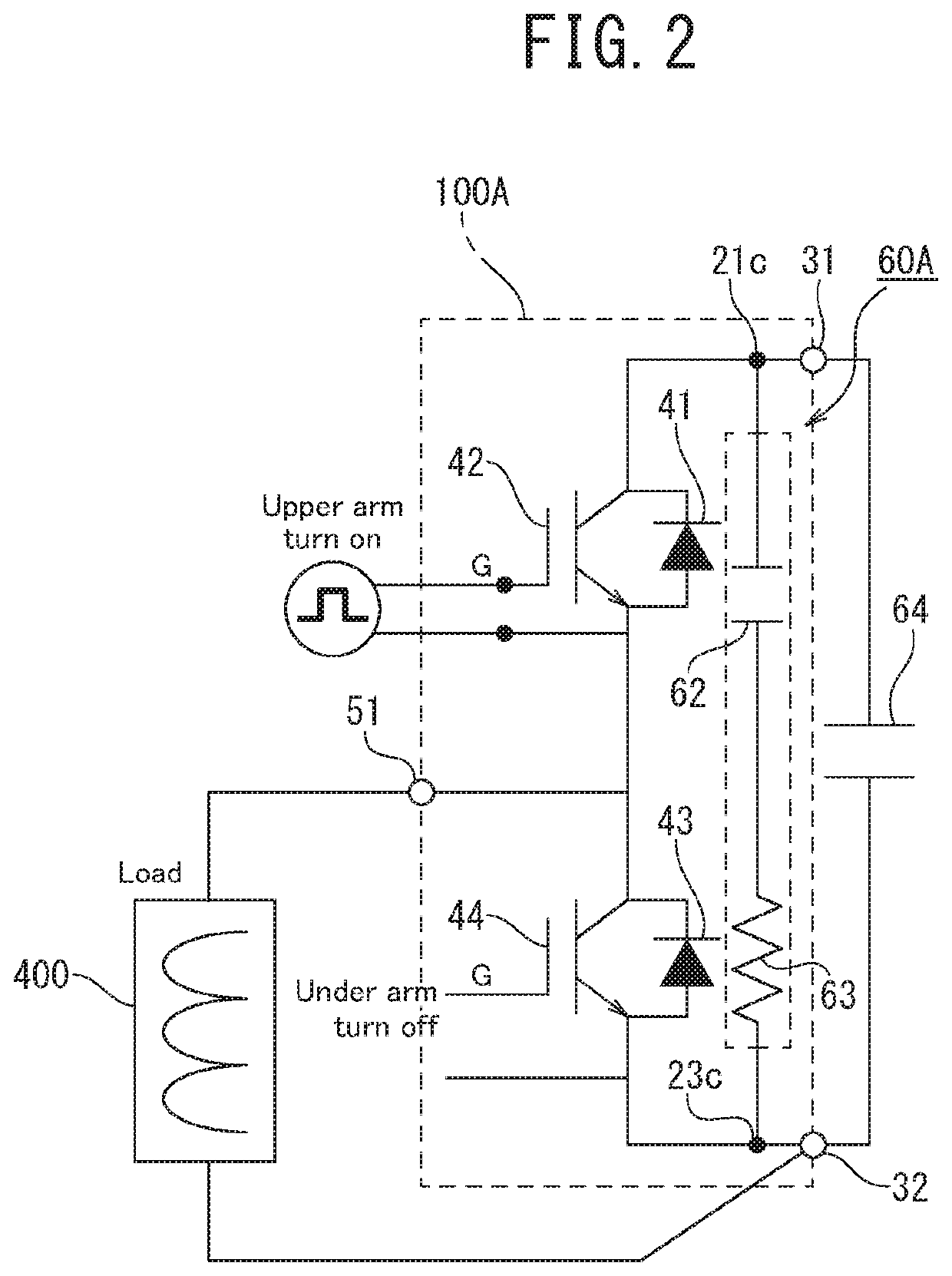
[0024]FIG. 1 is a schematic diagram of a top surface of a semiconductor module 100A according to a first embodiment of the present invention. As illustrated in FIG. 1, the semiconductor module 100A includes an insulating substrate 10, a switching element 42 as a first switching element, a switching element 44 as a second switching element, a copper plate 21 as a first metal plate, a copper plate 22 as a second metal plate, a copper plate 23 as a third metal plate, a copper plate 61 as a fourth metal plate, and a CR snubber circuit 60A including a capacitor 62 and a resistive wire 63.

[0025]The insulating substrate 10 may be any of a direct copper bonding (DCB) substrate, a direct bonded aluminum (DBA) substrate, an active metal brazing (AMB) substrate, and a metal-based plate, and the respective metal plates used can be a copper plate or an aluminum plate. The insulating substrate 10 according to the present embodiment is presumed to ...

second embodiment

[0052](Configuration of Semiconductor Module 100B)

[0053]FIG. 7 is a plan view illustrating a configuration of main parts of a semiconductor module 100B according to a second embodiment of the present invention. This embodiment uses copper plates as metal plates as in the case of the first embodiment. The semiconductor module 100B is provided with a slit elongated in the direction in which the mount part 23B extends (in the direction indicated by the arrow X2 in FIG. 7) at the boundary between the mount part 23A and the mount part 23B, and includes a narrow part 23d narrower than the negative-electrode terminal 32. The capacitor 62 is joined between the narrow part 21c and one end of the copper plate 61 (in the direction indicated by the arrow Y2 in FIG. 7). The resistive wire 63 is joined to the other end of the copper plate 61 (in the direction indicated by the arrow Y1 in FIG. 7) and the narrow part 23d.

[0054](Operational Effects of Semiconductor Module 100B)

[0055]The semiconduct...


PUM

PropertyMeasurementUnit
resistivityaaaaaaaaaa
ringing frequencyaaaaaaaaaa

Abstract

A semiconductor module includes: a first metal plate including a first mount part joined with a bottom-surface electrode of a first switching element, a second mount part joined with a positive-electrode terminal, and a first narrow part between the first and second mount parts and being narrower than a part jointing the first switching element to the first mount part and the positive-electrode terminal; a second metal plate being joined with a bottom-surface electrode of a second switching element, and connected to a top-surface electrode of the first switching element; a third metal plate including a sixth mount part joined with a negative-electrode terminal, a seventh mount part connected to a top-surface electrode of the second switching element, and being narrower than the negative-electrode terminal, and a second narrow part between the sixth and seventh mount parts; and a snubber circuit connecting the first and second narrow parts.

Description

CROSS-REFERENCE TO RELATED APPLICATION[0001]This application claims benefit of priority under 35 USC 119 based on Japanese Patent Application No. 2019-203152 filed on Nov. 8, 2019, the entire contents of which are incorporated by reference herein.BACKGROUND1. Field of the Invention[0002]The present invention relates to a semiconductor module and a method of manufacturing the semiconductor module.2. Description of the Related Art[0003]Semiconductor modules used for power conversion devices such as inverters typically include, as a switching element, a vertical integrated gate bipolar transistor (IGBT) or a metal-oxide-semiconductor field effect transistor (MOS-FET) provided on a silicon (Si) semiconductor substrate. To ensure high efficiency and high breakdown voltage, the use of wide bandgap semiconductors of silicon carbide (SiC) or gallium nitride (GaN) has been increased, and a MOS-FET mounted on a SiC semiconductor substrate is often used in recent years.[0004]A semiconductor mo...

Claims


Application Information

Patent Timeline
Patent Type & Authority Applications(United States)
IPC IPC(8): H01L27/02H02M1/34H01L29/16H01L23/12H01L21/66
CPCH01L27/0288H02M1/34H01L22/20H01L23/12H01L27/0255H01L29/1608H02M1/348H02M7/003H01L23/3735H01L23/5386H01L25/072H01L25/18H01L2224/37147H01L2224/40225H01L2224/41113H01L2224/49113H01L2224/45147H01L2224/45155H01L2224/4516H01L24/45H01L24/49H01L24/48H01L24/41H01L24/37H01L24/40H01L2224/45015H01L2224/48011H01L2924/19105H01L2924/19107H01L2924/19043H01L2924/19041H01L2924/30101H01L2924/00014H01L2924/01025H01L2924/01028H01L2924/01024H01L2924/01013H01L2924/20757H01L2924/20756H01L2924/20758H01L2224/73221H01L23/642H01L23/647H01L23/492H01L23/49838H01L28/40H01L28/20H01L23/4824
Inventor NAKANO, HAYATO
Owner FUJI ELECTRIC CO LTD
Why Eureka
Try Eureka