
Organic light-emitting diode display device and driving method thereof

a light-emitting diode display and organic technology, applied in the direction of instruments, static indicating devices, etc., can solve the problems of low light-emission efficiency of pdp, large power consumption, motion blurring, etc., to reduce residual image phenomenon, reduce motion image blurring phenomenon, and reduce display deterioration

Active Publication Date: 2010-07-06
LG DISPLAY CO LTD
View PDF12 Cites 24 Cited by
  • Summary
  • Abstract
  • Description
  • Claims
  • Application Information

AI Technical Summary

Benefits of technology

The invention is an organic light-emitting diode display device and a driving method thereof that address various limitations and disadvantages of existing technology. The technical effects of the invention include reducing display deterioration caused by a thin film transistor having hysteresis, reducing residual image phenomenon, reducing motion image blurring, and compensating voltage drops in the driving voltage and ground voltage supply line. These improvements enhance the performance and quality of the organic light-emitting diode display device.

Problems solved by technology

However, a PDP has a low light-emission efficiency and requires large power consumption.
Likewise, an active matrix LCD device employing a thin film transistor (hereinafter, referred to as “TFT”) as a switching device has experienced drawbacks in that it is difficult to make a large dimension screen because a semiconductor process is used, but has an expanded demand as it is mainly used for a display device of a notebook personal computer.
Thus, brightness of each pixel for one frame period is maintained, thereby burring an image of a motion picture and causing motion blurring.
This phenomenon worsens as the driving voltage line VL becomes longer in a large size panel.

Method used


Image

  • Organic light-emitting diode display device and driving method thereof
  • Organic light-emitting diode display device and driving method thereof
  • Organic light-emitting diode display device and driving method thereof

Examples


Embodiment Construction

[0062]Reference will now be made in detail to the preferred embodiments of the invention, examples of which are illustrated in the accompanying drawings.

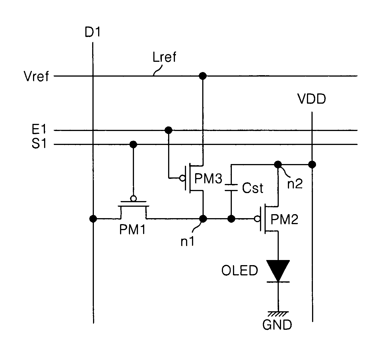
[0063]FIG. 8 is a block diagram illustrating an organic light-emitting diode display device according to an embodiment of the invention. In FIG. 8, an organic light-emitting diode display device includes a display panel 80, a data driving device 82, a scan driving device 83, and a timing controller 81. The display panel 80 has m data lines DL1 to DLm, n first scan lines S1 to Sn, n second scan lines E1 to En, and m×n pixels 84. The data driving device 82 supplies a data voltage to the data lines DL1 to DLm. The scan driving device 83 sequentially supplies a first scanning pulse to the first scan lines S1 to Sn, and sequentially supplies a second scanning pulse to the second scan lines E1 to En. The timing controller 81 controls the data driving device 82 and the scan driving device 83.

[0064]In addition, the pixels 84 are formed at p...


PUM


Abstract

An organic light-emitting diode display device includes a first switch element turned-on in response to a first scanning signal during a first period to supply a data to a first node, and then maintaining an off-state during a second period, a driving device adjusting a current through an organic light-emitting diode element in accordance with a voltage of the first node; a reference voltage source providing a reference voltage that is capable of turning-off the driving device, a second switch element maintaining an off-state during the first period, and turned-on during the second period to supply the reference voltage to the first node, and a storage capacitor maintaining the voltage at the first node.

Description

[0001]The invention claims the benefit of Korean Patent Application No. P06-0056566 filed in Korea on Jun. 22, 2006, which is hereby incorporated by reference in its entirety.BACKGROUND OF THE INVENTION[0002]1. Field of the Invention[0003]The invention relates to an organic light-emitting diode display device, and more particularly, to an organic light-emitting diode display device and a driving method thereof. Although embodiments of the invention are suitable for a wide scope of applications, they are particularly suitable for reducing a residual image phenomenon and a motion image blurring phenomenon, and for compensating a voltage drop of a driving voltage in an organic light-emitting diode display device.[0004]2. Discussion of the Related Art[0005]Recently, flat display panels with reduced weight and size have been developed to eliminate disadvantages of a cathode ray tube display device. Such flat panel display devices include a liquid crystal display (hereinafter, referred to...

Claims


Application Information

Patent Timeline
Patent Type & Authority Patents(United States)
IPC IPC(8): G09G3/32
CPCG09G3/3233G09G2300/0842G09G2310/0251G09G2320/0261G09G2310/061G09G2320/0233G09G2310/06G09G3/30G09G3/20
Inventor KIM, O HYUNCHUNG, HOON JUJUNG, MYOUNG HOON
Owner LG DISPLAY CO LTD
Learn More