Display device and method of producing the same

a display device and display technology, applied in the field of display devices, can solve the problems of affecting crystallization, lowering the display quality of the active matrix display device, and high resistance of the polycrystalline semiconductor film, so as to achieve the effect of improving the display quality of the display devi

Active Publication Date: 2010-07-13
TRIVALE TECH
View PDF14 Cites 5 Cited by
  • Summary
  • Abstract
  • Description
  • Claims
  • Application Information

AI Technical Summary

Benefits of technology

[0016]The invention has been conducted in order to solve above-discussed problems. It is an object of the invention to, in a display device comprising a storage capacitor having a semiconductor film, and a thin film transistor, form the storage capacitor so that it does not depend on the voltage, without adversely affecting a high-temperature treatment on the semiconductor film, thereby improving the display quality of the display device.
[0018]In the display device of the invention, the conductive film is stacked above the polycrystalline semiconductor film which is a lower electrode of the storage capacitor. Therefore, a desired capacitance corresponding to the thickness of the insulating film can be obtained, and the display quality of the display device can be improved.

Problems solved by technology

Hence, there is a problem in which a resistance of the polycrystalline semiconductor film is high.
Therefore, a large problem arises when, for example, a wiring is drawn from the TFT to the storage capacitor.
Furthermore, a voltage dependency due to the property of the semiconductor possessed by the polycrystalline semiconductor film itself is produced.
Consequently, there is a further problem in that a desired capacitance corresponding to the thickness of the insulating film cannot be obtained, and the display quality of the active matrix display device is lowered.
In the crystallization of a semiconductor film by a high-temperature treatment using a laser beam or the like, however, the conductive film adversely affects the crystallization, and a polycrystalline semiconductor film of the high quality cannot be obtained.
In the view of this point, the technique is not practical (for example, see Patent Reference 4).

Method used


Image

  • Display device and method of producing the same
  • Display device and method of producing the same
  • Display device and method of producing the same

Examples


embodiment 1

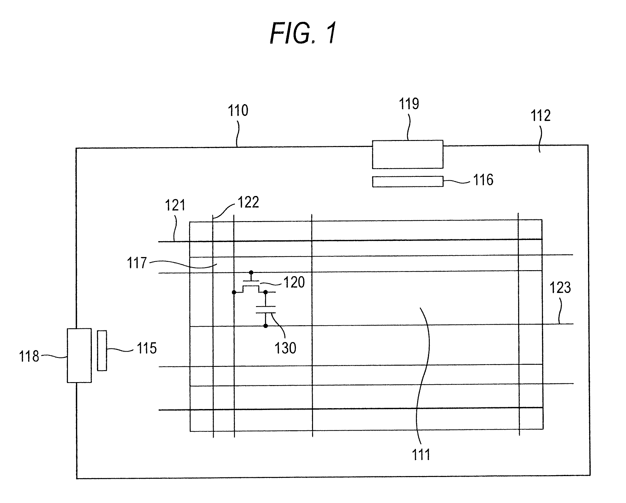
[0031]First, a TFT substrate constituting the display device of the invention will be described. FIG. 1 is a front view showing the configuration of a TFT substrate used in the display device. As the display device of the invention, a liquid crystal display device will be exemplarily described. However, this is for illustrative purpose only. Alternatively, for example, a flat panel display device such as an organic EL display device may be used.

[0032]The display device of the invention has the TFT substrate 110. For example, the TFT substrate 110 is a TFT array substrate. In the TFT substrate 110, a display region 111, and a frame region 112 which surrounds the display region 111 are disposed. In the display region 111, plural gate wirings (scan signal lines) 121 and plural source wirings (display signal lines) 122 are formed. The plural gate wirings 121 are disposed in parallel to one another. Similarly, the plural source wirings 122 are disposed in parallel to one another. The gat...

embodiment 2

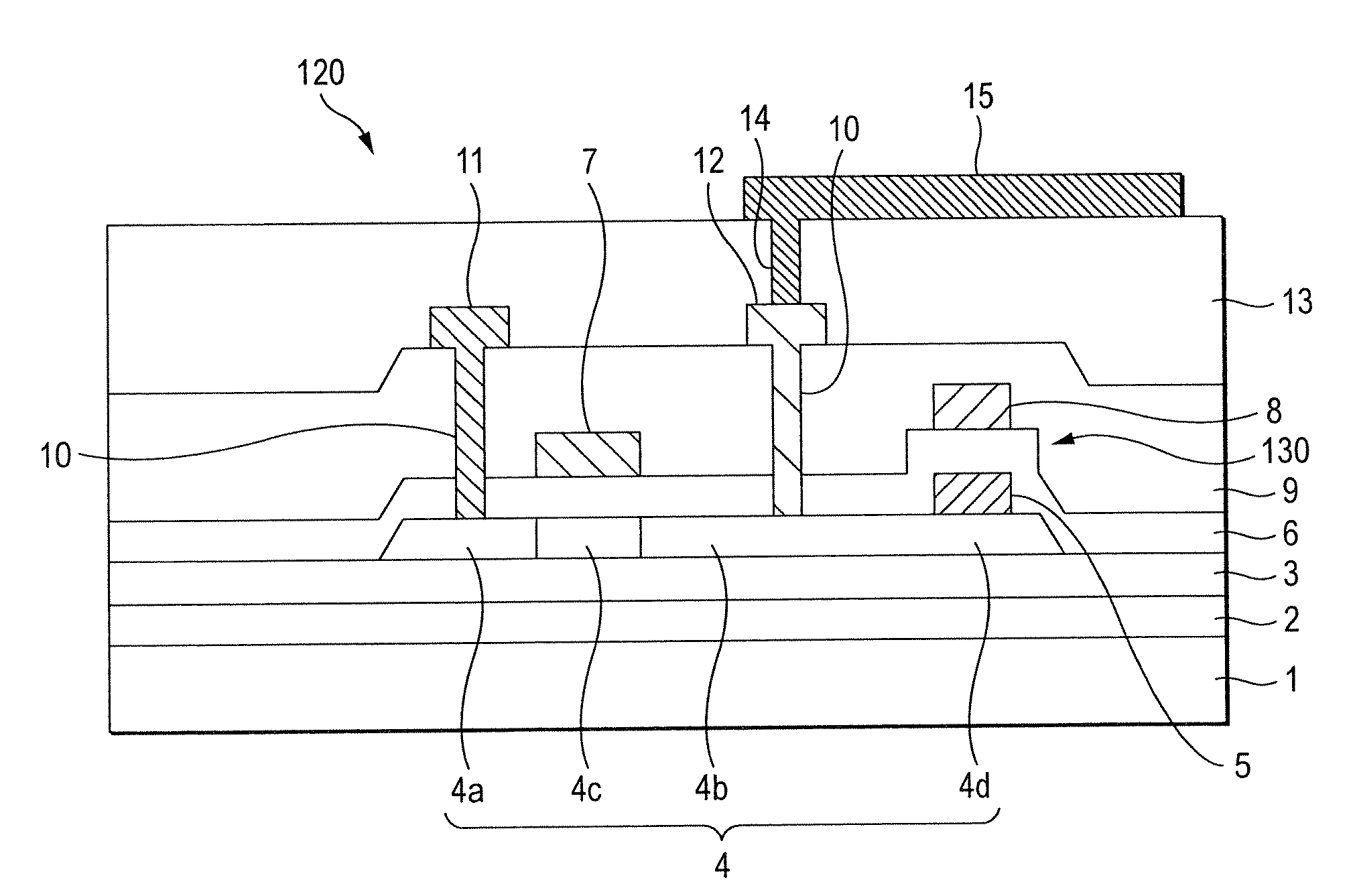
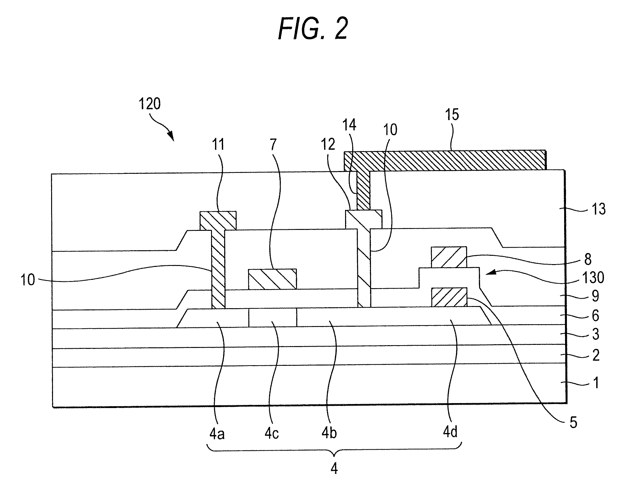
[0067]In Embodiment 1, the conductive film was formed only on the storage capacitor lower portion which is a semiconductor layer for forming the lower electrode of the storage capacitor. Embodiment 2 is characterized in that the conductive film which is to be formed on the semiconductor layer is formed not only in the storage capacitor, but also in a portion which is contacted to the drain electrode in the drain region, and that which is contacted to the source electrode in the source region. FIG. 8 is a sectional view of the TFT120 and the storage capacitor 130 in a display device of Embodiment 2.

[0068]Referring to FIG. 8, the conductive film 5 is extended from the storage capacitor 130 so as to be formed not only therein, but also on the drain region 4b of the TFT 120. Furthermore, the conductive film is formed also on the source region 4a. Namely, as the conductive film 5, there are not only the conductive film formed as the storage capacitor 130, but also the conductive film 5 f...

embodiment 3

[0071]FIG. 9 is a sectional view of the TFT 120 and the storage capacitor 130 in the display device of Embodiment 3. Embodiment 3 is different from Embodiments 1 and 2 in that the first contact holes 10 formed in the gate insulating film 6 and the first interlayer insulating film 9, and the second contact hole 14 formed in the second interlayer insulating film 13 are overlappingly formed at a substantially same position, and that the pixel electrode 15 and the conductive film 5 are directly connected to each other without passing through the drain electrode 12. The production method is different only in the existence / nonexistence of the drain electrode 12, and the timing of the formation of the first contact holes 10. In Embodiment 2, the first contact holes 10 are opened after the first interlayer insulating film 9 is formed. By contrast, Embodiment 3 is characterized in that, after the second interlayer insulating film 13 is formed, the second contact hole 14 and the first contact...


PUM


Abstract

In a thin film transistor using a polycrystalline semiconductor film, when a storage capacitor is formed, it is often that a polycrystalline semiconductor film is used also in one electrode of the capacity. In a display device having a storage capacitor and thin film transistor which have a polycrystalline semiconductor film, the storage capacitor exhibits a voltage dependency due to the semiconductor film, and hence a display failure is caused. In the display device of the invention, a metal conductive film 5 is stacked above a semiconductor layer 4d made of a polycrystalline semiconductor film which is used as a lower electrode of a storage capacitor 130.

Description

CROSS-REFERENCE TO RELATED APPLICATION[0001]This application is based upon and claims the benefit of priority from Japanese Patent Application No. 2006-330528 filed on Dec. 7, 2006, the entire contents of which are incorporated herein by reference.BACKGROUND OF THE INVENTION[0002]1. Field[0003]The present invention relates to a display device, and particularly to a structure of an active matrix display device comprising a thin film transistor and a storage capacitor, and also to a method of producing it.[0004]2. Description of the Related Art[0005]A liquid crystal display device (LCD) which is one of conventional usual thin panels is generally used as a monitor for a personal computer, that for a portable information terminal, and the like, while taking advantage of low power consumption, small size, and light weight. Recently, such a device is widely used in a TV set, and will replace a conventional cathode-ray tube. Also an electroluminescence EL display device in which a luminous...

Claims


Application Information

Patent Timeline
Patent Type & Authority Patents(United States)
IPC IPC(8): H01L21/00
CPCH01L27/1288H01L27/1255H01L28/60G02F1/136213G02F1/136227G02F1/136
Inventor TAKEGUCHI, TORUIMAMURA, TAKUJIYAMAYOSHI, KAZUSHIIRIZUMI, TOMOYUKINISHIURA, ATSUNORIMOTONAMI, KAORU
Owner TRIVALE TECH
Why Eureka
Try Eureka