

Scanning electron microscope
a scanning electron microscope and electron microscope technology, applied in the field of scanning electron microscope, can solve the problem of high price of detector typ
- Summary
- Abstract
- Description
- Claims
- Application Information
AI Technical Summary
Benefits of technology
Problems solved by technology
Method used
Image

Examples
embodiment 1
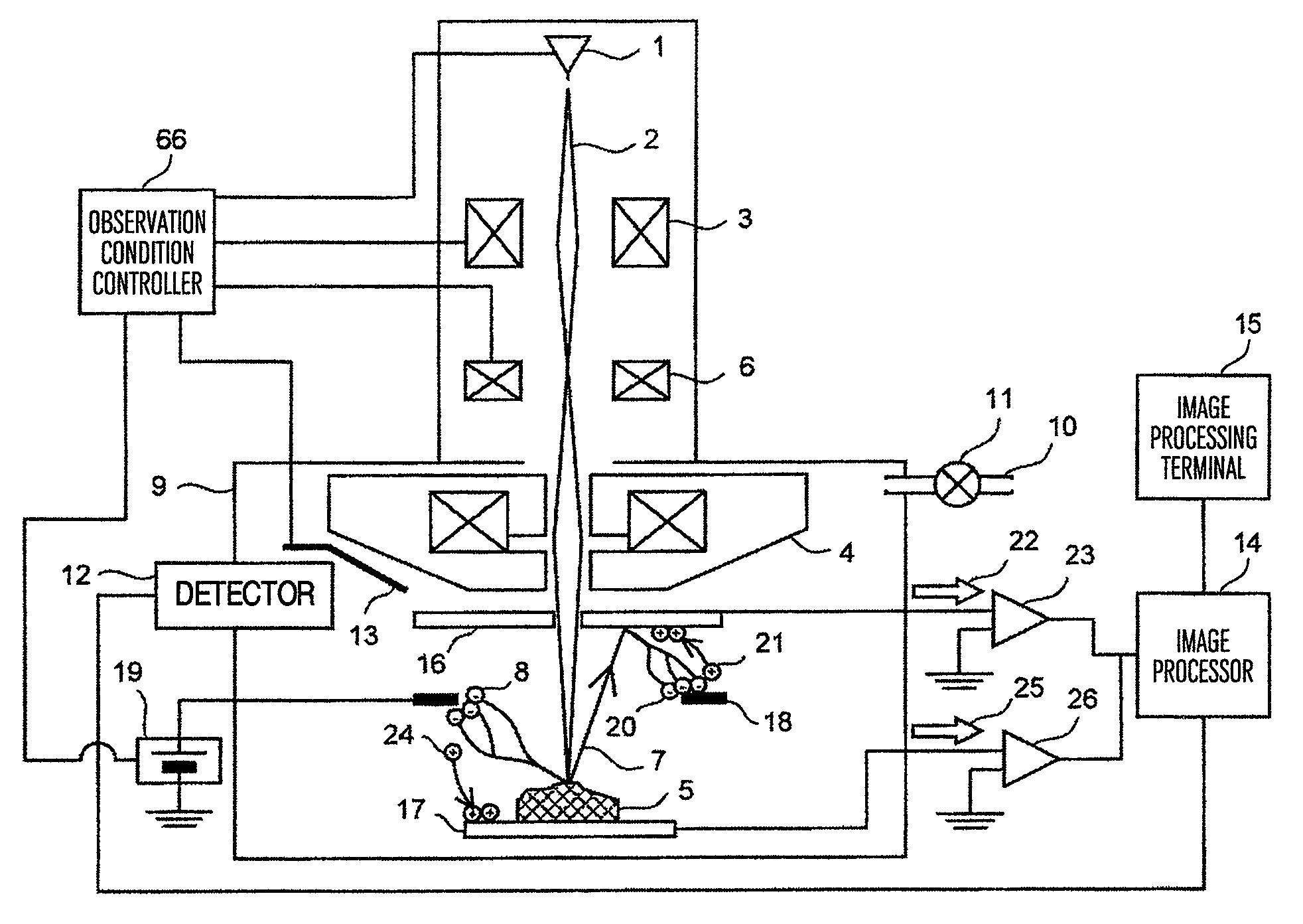
[0046]In the present embodiment as will be described hereunder, a scanning electron microscope capable of acquiring both low vacuum secondary electron image and low vacuum backscattering electron image comprises a backscattering electron detection electrode which is arranged near the illuminating optical axis of a primary electron beam, that is, a so-called on-axis detection type backscattering electron detection electrode and the backscattering electron detection electrode is also used as a reflection plate.
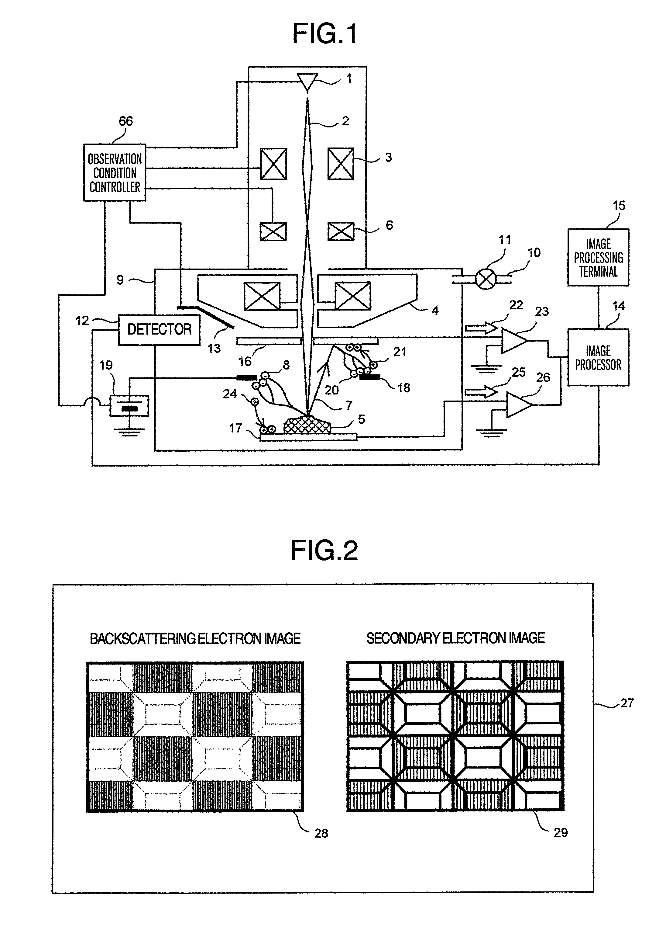
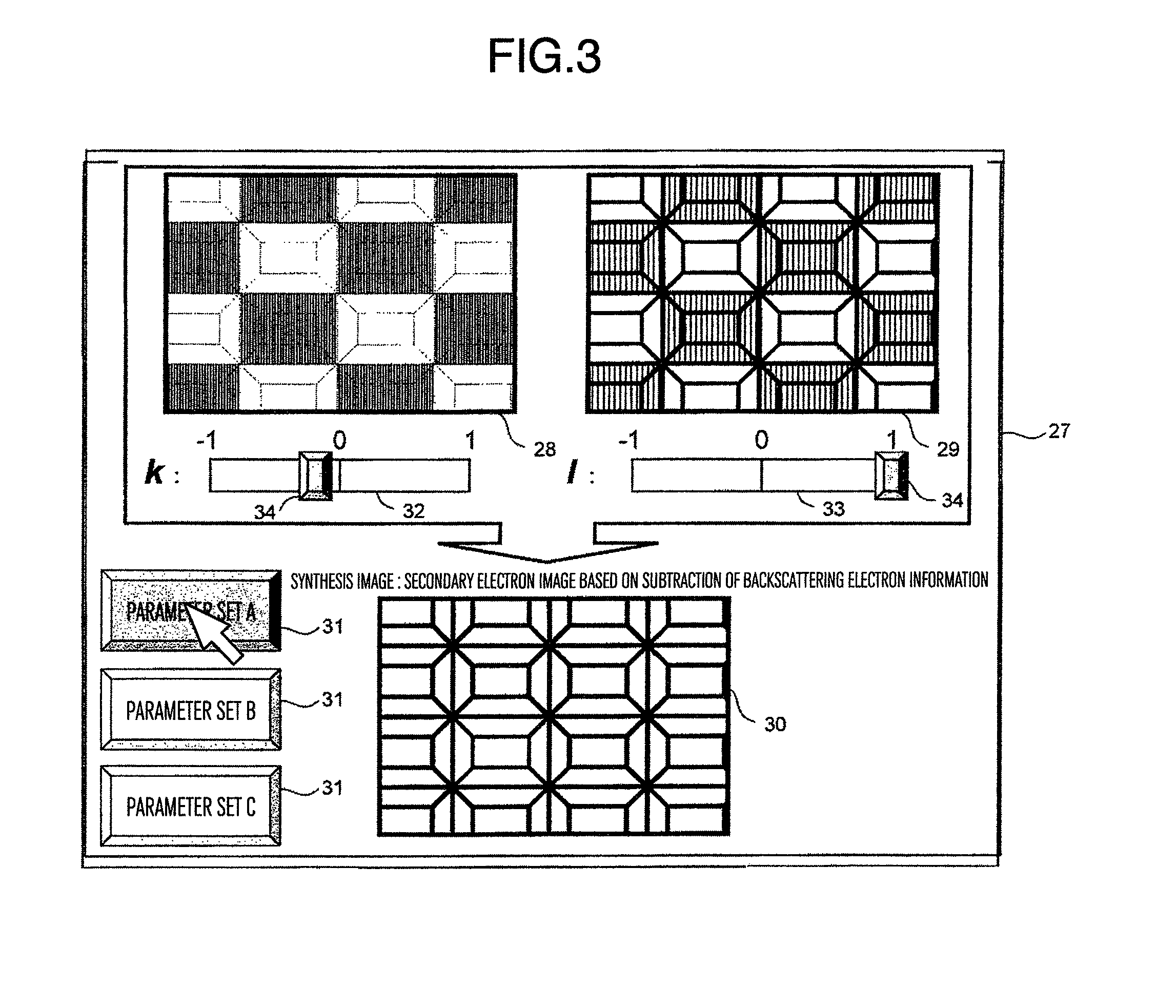
[0047]Referring to FIG. 1, in a low vacuum SEM having an on-axis detection type backscattering electron detection means in the form of a reflection plate and detection electrode, a secondary electron detection means is arranged on a specimen stage or in the vicinity thereof as schematically illustrated. The scanning electron microscope as shown in FIG. 1 comprises an electron optics column, a specimen chamber 9, an image processor 14 for processing signals indicative of ion curr...
embodiment 2
[0086]The embodiment using the on-axis backscattering electron detection type and using backscattering electron detection electrode and reflection plate in common has been described in connection with embodiment 1 but in embodiment 2, an embodiment also being of the on-axis detection type but not using the backscattering electron detection electrode and the reflection plate in common will be described.
[0087]Referring to FIG. 9, a construction example of the present embodiment will be described. A scanning electron microscope in the FIG. 9 construction example is the same as the apparatus of FIG. 1 construction example with the exception that a disk-shaped detection electrode 61 for backscattering electron detection in the form of a doughnut is arranged in a space between reflection plate 16 and specimen stage 17. Unlike the individual construction examples explained in connection with embodiment 1, the reflection plate is grounded. With a view to promoting the efficiency of detectio...
embodiment 3
[0095]While, in the embodiments 1 and 2, apparatuses analogous to the on-axis detection type apparatus have been explained, an embodiment in which the present invention is applied to a scanning electron microscope of off-axis detection type will now be described. The off-axis detection is a technical term in contrast to the on-axis detection and signifies a detection scheme in which in contrast to the on-axis detection for detecting backscattering electrons reflected in a direction making a relatively small azimuth angle to the optical axis of electron beam 2 (high angle backscattering electrons), backscattering electrons reflected in a direction making a large azimuth angle to the optical axis (low angle backscattering electrons) are detected off-axially by means of a detector arranged obliquely to the optical axis.
[0096]Referring to FIG. 13, an example of the most basic construction for separating and detecting low vacuum secondary electrons and low vacuum backscattering electrons...
PUM
 Abstract
Description
Claims
Application Information