Dummy active area implementation

a technology of active area and dummy, which is applied in the direction of semiconductor devices, basic electric elements, electrical equipment, etc., can solve the problems of significant man hours required to design such scaled-down devices, significant cost associated with exercising quality control over semiconductor fabrication, and high equipment costs. achieve the effect of reducing yield loss and more uniformity

Active Publication Date: 2010-07-20
TEXAS INSTR INC
View PDF9 Cites 4 Cited by
  • Summary
  • Abstract
  • Description
  • Claims
  • Application Information

AI Technical Summary

Benefits of technology

[0006]Areas of a semiconductor substrate where semiconductor devices are not to be formed are filled in with dummy active areas. Whole dummy active areas are formed in areas of the semiconductor substrate where semiconductor devices are not to be formed, and partial dummy active areas are formed in areas of the semiconductor substrate where semiconductor devices are not to be formed, but where whole dummy active areas can not be accommodated. The dummy active areas are substantially evenly separated from one another by dividers. The dummy active areas and dividers are formed concurrently with formation of semiconductor devices in non-dummy active areas. The dummy active areas mitigate yield loss by providing more uniformity across the substrate, at least with regard to parasitic capacitances and subsequent processing.

Problems solved by technology

For example, significant man hours may be required to design such scaled down devices, equipment necessary to produce such devices may be expensive and / or processes related to producing such devices may have to be very tightly controlled and / or be operated under very specific conditions, etc.
Accordingly, it can be appreciated that there can be significant costs associated with exercising quality control over semiconductor fabrication, including, among other things, costs associated with discarding defective units, and thus wasting raw materials and / or man hours, as well as other resources, for example.
Additionally, since the units are more tightly packed on the wafer, more units are lost when some or all of a wafer is defective and thus has to be discarded.

Method used


Image

  • Dummy active area implementation
  • Dummy active area implementation
  • Dummy active area implementation

Examples


Embodiment Construction

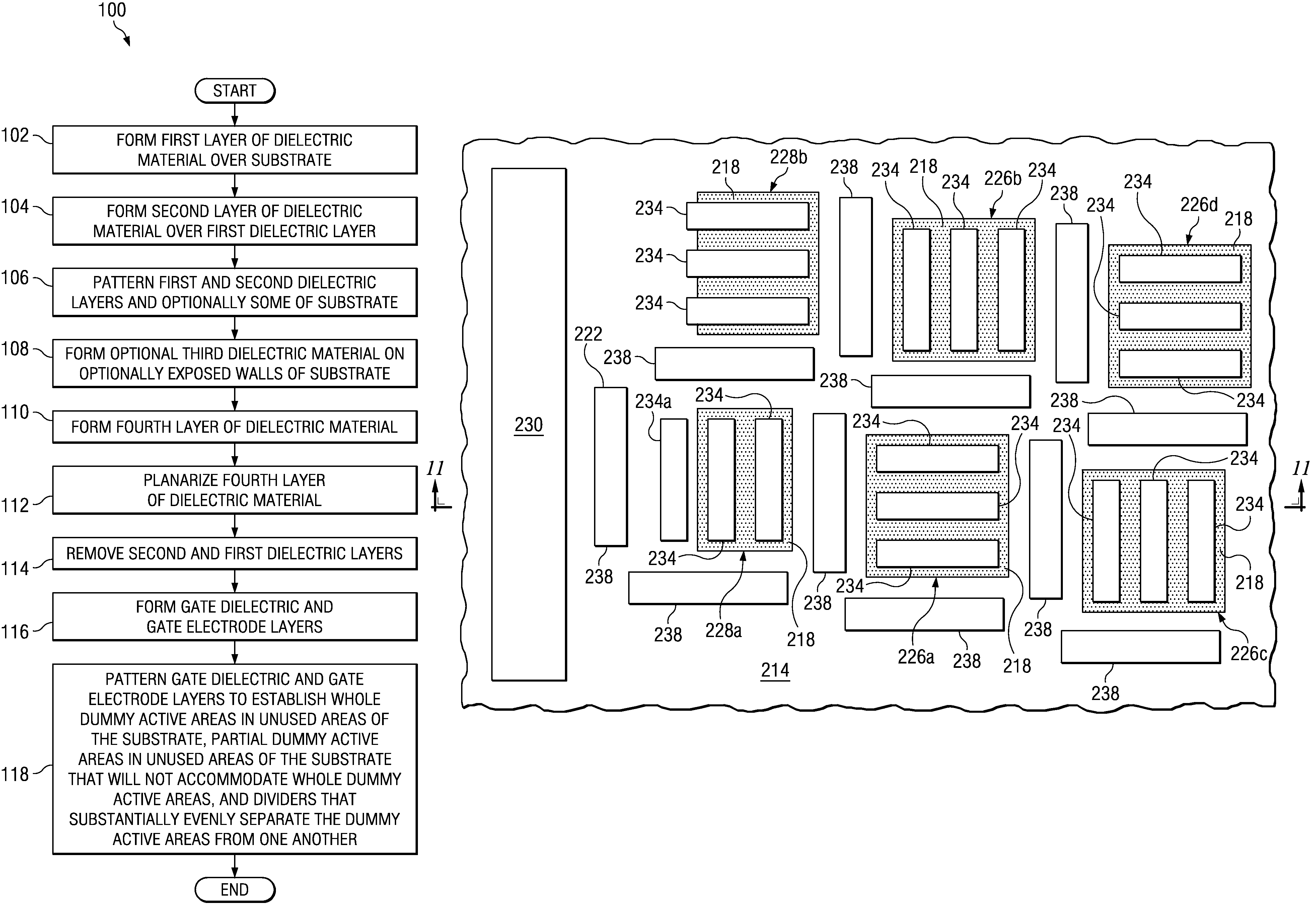
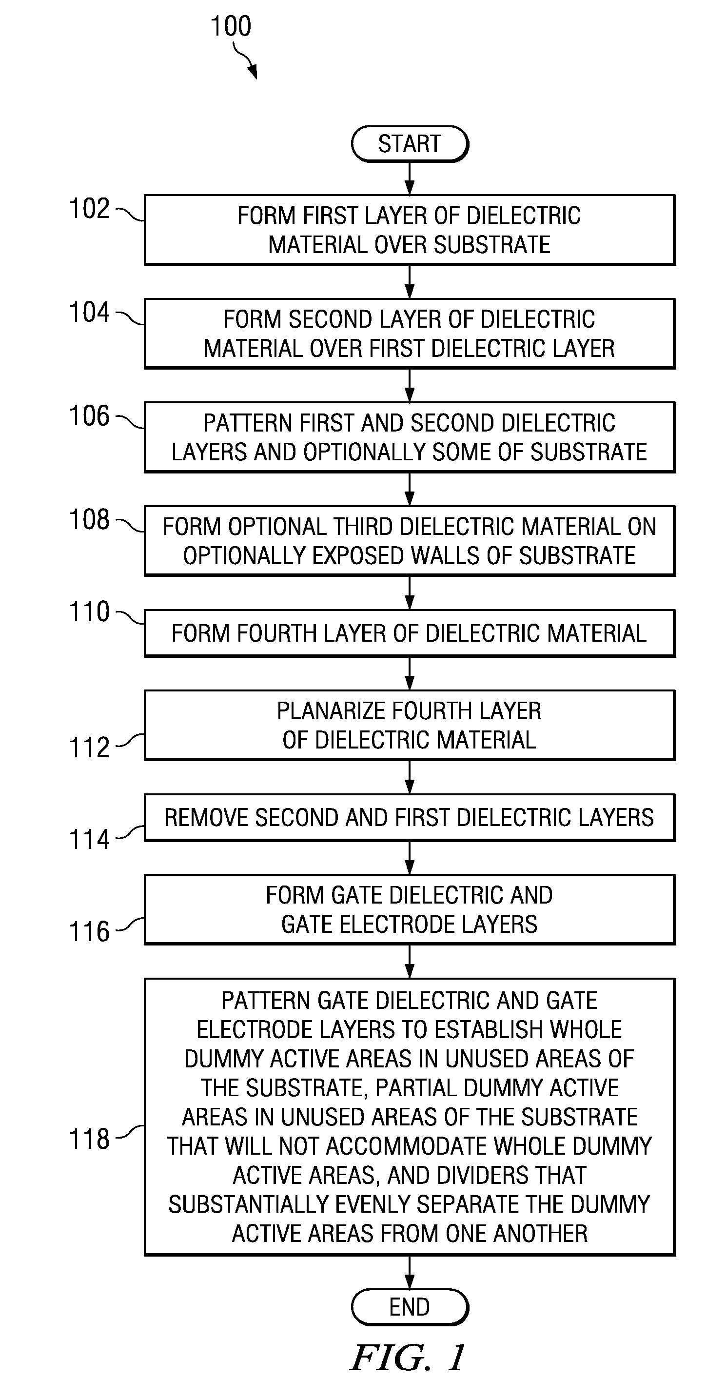
[0011]The description herein is made with reference to the drawings, wherein like reference numerals are generally utilized to refer to like elements throughout, and wherein the various structures are not necessarily drawn to scale. In the following description, for purposes of explanation, numerous specific details are set forth in order to provide a thorough understanding. It may-be evident, however, to one skilled in the art, that one or more aspects described herein may be practiced with a lesser degree of these specific details. In other instances, known structures and devices are shown in block diagram form to facilitate a thorough understanding.

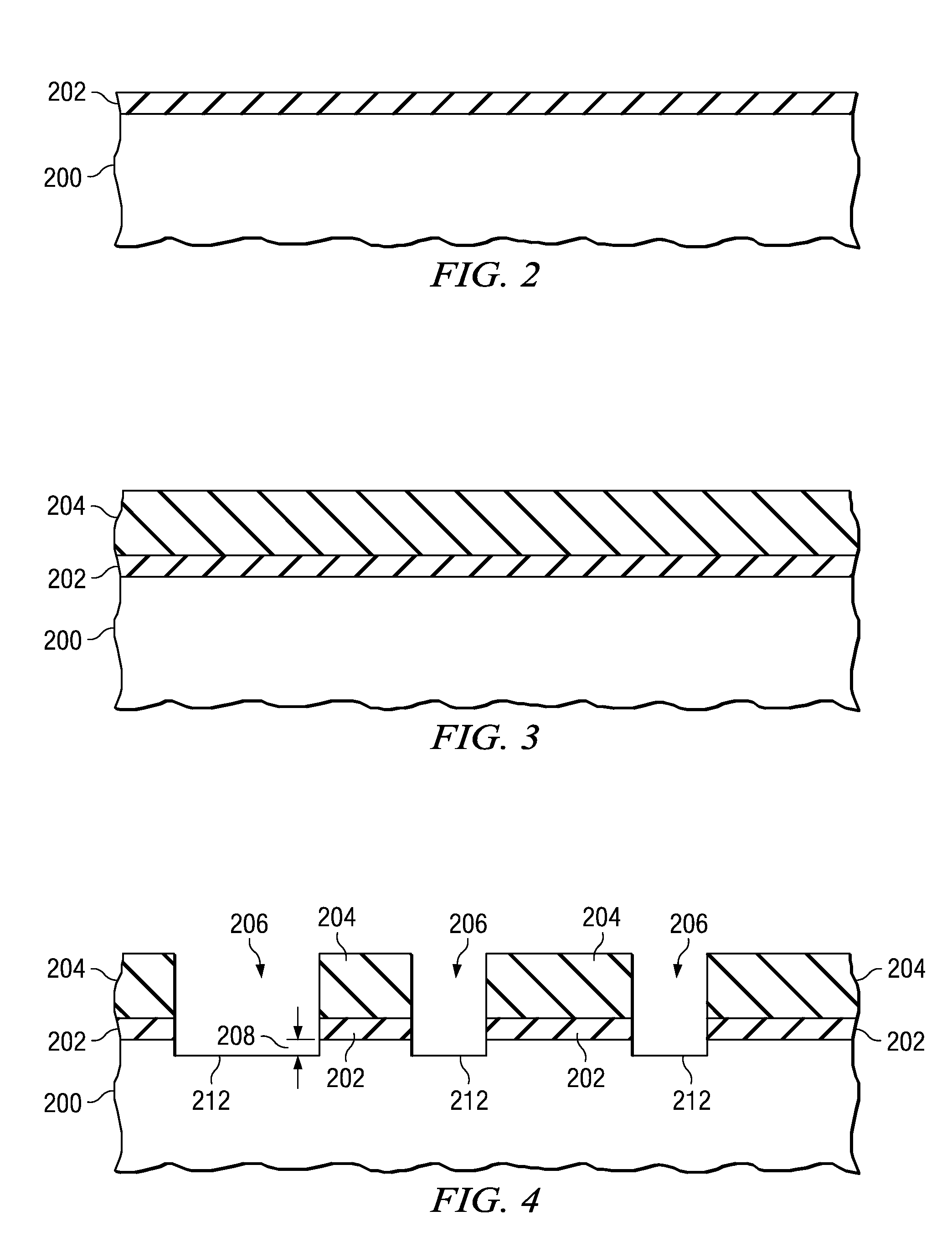
[0012]An example methodology 100 for filling in areas of a semiconductor substrate where semiconductor devices are not to be formed as described herein is illustrated in FIG. 1, and an example semiconductor substrate where areas of the substrate 200 that are not to include semiconductor devices are filled in with dummy active areas as ...


PUM


Abstract

Areas of a semiconductor substrate where semiconductor devices are not to be formed are filled in with dummy active areas. Whole dummy active areas are formed in areas of the semiconductor substrate where semiconductor devices are not to be formed, and partial dummy active areas are formed in areas of the semiconductor substrate where semiconductor devices are not to be formed, but where whole dummy active areas can not be accommodated. The dummy active areas are staggered so as to provide uniform parasitic capacitive coupling to overlying leads regardless of the placement of the leads. The dummy active areas are substantially evenly separated from one another by dividers. The dummy active areas and dividers are formed concurrently with formation of semiconductor devices in non-dummy active areas. The dummy active areas mitigate yield loss by, among other things, providing more uniformity across the substrate, at least with regard to parasitic capacitances and stress and subsequent processing.

Description

FIELD OF THE INVENTION[0001]The present invention relates generally to semiconductor processing, and more particularly to forming dummy active areas in areas of a semiconductor substrate where semiconductor devices are not to be formed.BACKGROUND OF THE INVENTION[0002]Several trends presently exist in the semiconductor and electronics industry. Devices are continually being made smaller, faster and requiring less power. One reason for these trends is that more personal devices are being fabricated that are relatively small and portable, thereby relying on a battery as their primary supply. For example, cellular phones, personal computing devices, and personal sound systems are devices that are in great demand in the consumer market. In addition to being smaller and more portable, personal devices are also requiring increased memory and more computational power and speed. In light of all these trends, there is an ever increasing demand in the industry for smaller and faster transisto...

Claims


Application Information

Patent Timeline
Patent Type & Authority Patents(United States)
IPC IPC(8): H01L21/338
CPCH01L27/0207
Inventor FLECK, ROBERT G.OLSEN, LEIF C.TIGELAAR, HOWARD L.
Owner TEXAS INSTR INC
Why Eureka
Try Eureka