Formation of contacts on semiconductor substrates

a technology of semiconductor substrates and contacts, applied in the direction of radioation control devices, television system scanning details, television systems, etc., can solve problems such as certain characteristics of conductive contacts, and achieve the effects of reducing inter-contact resistivity, stable performance, and increasing surface leakage curren

Inactive Publication Date: 2010-08-03
SIEMENS AG
View PDF76 Cites 0 Cited by
  • Summary
  • Abstract
  • Description
  • Claims
  • Application Information

AI Technical Summary

Benefits of technology

[0012]In one arrangement the first layer is a contact layer and the second layer is a diffusion barrier layer, which means that embodiments can provide particularly good chemical contact with the substrate (via the contact layer) and improved lifetime (via the diffusion barrier layer). In some embodiments the conductive contacts additionally include either or both of a third conductive layer and a further conductive layer, the third being sandwiched between the first and second layers and the further being adjacent the second layer. The third layer acts as an adhesion layer, whilst the further layer acts as a wetting agent for the bump bonding. Advantageously, the diffusion barrier (second) layer prevents bump bond material (e.g. PbSnBi solder) from diffusing into layers beyond the diffusion barrier layer, which is detrimental to the lifetime of the detector.
[0013]Preferably, the conductive layers are applied by methods such as sputtering, evaporation, electrolytic deposition, or electroless deposition (e.g. chemical deposition), before any subsequent layers are formed. An advantage of forming the plurality of contiguous layers of conductive materials first (i.e. before applying an insulating layer such as a passivation layer) is that this can improve electrical contact characteristics, reduce hotspots, improve yield and improve detector quality. Homogenous contacts with even electrical contacts can thus be reliably produced.
[0019]The surface resistivity of cadmium-based substrates in particular, for example a CdZnTe semiconductor substrate, is degraded when the substrate is exposed to metal etchants suitable for removing gold and / or platinum, for example. As a result of this, the electrical separation of the individual contacts which result from some known methods of forming such contacts is not as good as would be expected from the properties of that material before treatment. By using a lift-off method in accordance with the invention, metal etchants need not be used, thus avoiding the damage which would result if the metal etchants came into contact with the semiconductor surface.
[0023]An advantage of applying the further layer of photoresistive material is that areas of varying size, specifically, smaller or larger than the contact positions, can be exposed, which means that portions of the layer of passivation material can be removed from areas smaller than the conductive contacts. After this removal of portions of said passivation layer, the passivation material can overlap with the conductive contacts. This means that the passivation material may be applied over portions of the conductive contacts, providing good mechanical contact, and reducing the possibility of gaps being formed between the conductive material and passivation material.
[0032]Preferably the radiation detector includes an electrically insulating passivation layer between contacts distributed on the semiconductor substrate, which enables the area between metal contacts to be protected, thus giving the detector stable performance over time and avoiding effects such as oxidation which increase the surface leakage current and decrease the inter-contact resistivity. Aluminium nitride (AlN) passivation has been found to be particularly effective when applied between gold contacts to protect the surface and enhance the electrical separation of the gold contacts. The passivation layer of aluminium nitride can be implemented at relatively low temperatures typically less than 100° C. By contrast, silicon oxide (SiO2), which is typically used as a passivant for silicon (Si) semiconductors, needs temperatures in excess of 200° C. After exposure to these temperatures, CdZnTe would be unusable.
[0033]Embodiments in accordance with the present invention may be used to define areas or regions away from, yet operatively related to, contact positions. This is particularly advantageous and is intended for use in manufacturing high energy (IKeV) radiation imaging devices since it allows more complex conductive material patterns to be formed (e.g. for spatially off-setting a charge collection contact of a detector cell relative to a corresponding contact of a read-out substrate cell).

Problems solved by technology

In some known radiation detectors, problems have been observed with certain characteristics of the conductive contacts.

Method used


Image

  • Formation of contacts on semiconductor substrates
  • Formation of contacts on semiconductor substrates
  • Formation of contacts on semiconductor substrates

Examples


example 2

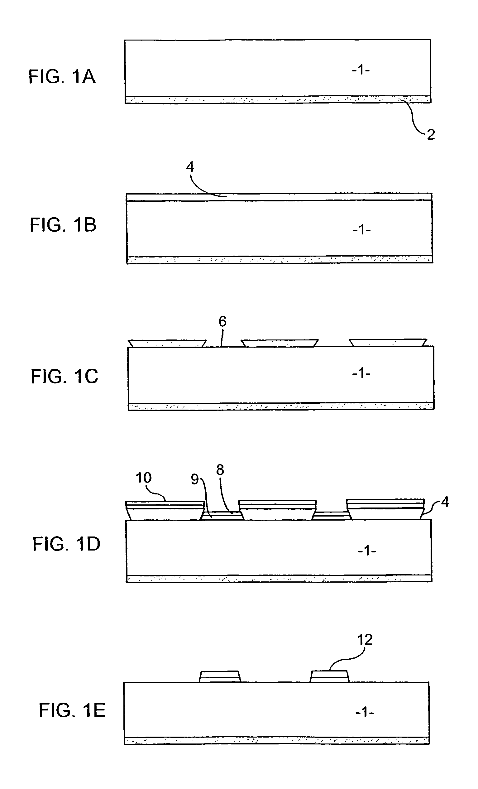
[0058]Referring to FIG. 2A, cadmium zinc telluride or cadmium telluride is used as the semiconductor substrate 1, and an indium metallisation layer is used as the conductive material 2 on the lower face of the detector in step A. The conductive layers 8, 9 in step D form a stack of platinum, gold, nickel and gold. The passivation material 14 in step F is sputtered aluminium nitride formed by phase vapour deposition. In step I alkali solution is used to etch the aluminium nitride.

[0059]The end result is a cadmium zinc telluride / cadmium zinc substrate 40, an aluminium nitride passivation layer 44 and conductive contacts formed as a stack of platinum, gold, nickel and gold 45, 46, 47, 48.

example 3

[0060]This example corresponds to Example 2 except that the conductive contacts are formed as a stack of platinum 45, gold 46, indium 47 and gold 48.

example 4

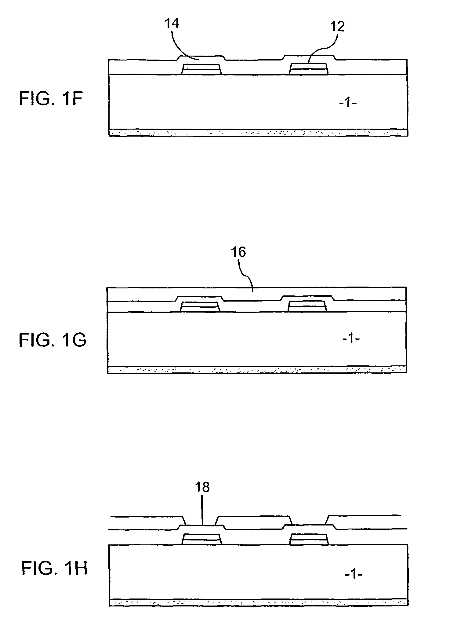
[0061]Referring to FIG. 2B, cadmium zinc telluride or cadmium telluride is used as the semiconductor substrate 1, and a platinum metallisation layer is used as the conductive material 2 on the lower face of the detector in step A. The conductive layers 8, 9 in step D comprise a stack of nickel and gold. The passivation material 14 in step F is sputtered aluminium nitride formed by phase vapour deposition. In step I alkali solution is used to etch the aluminium nitride.

[0062]The end result comprises a cadmium zinc telluride / cadmium zinc substrate 50, a platinum layer 52, an aluminium nitride passivation layer 54 and conductive contacts formed as a stack of nickel 55 and gold 56.

[0063]In other examples, stacks of platinum / gold / nickel; platinum / gold; indium / gold; chrome / copper / gold and platinum / titanium-tungsten alloy / gold are used.

[0064]Embodiments of the invention produce a detector with a lower face having a uniform conductive layer (e.g. a metallised layer such as a gold layer) and...


PUM


Abstract

Embodiments of the invention are concerned with a method of manufacturing a radiation detector having one or more conductive contacts on a semiconductor substrate, and comprise the steps of: applying a first conductive layer to a first surface of the semiconductor substrate; applying a second conductive layer to form a plurality of contiguous layers of conductive materials, said plurality of contiguous layers including said first conductive layer; and selectively removing parts of said plurality of contiguous layers so as to form said conductive contacts, the conductive contacts defining one or more radiation detector cells in the semiconductor substrate.

Description

[0001]This is a 371 national phase application of PCT / GB2003 / 004577 filled 23 Oct. 2003, claiming priority to GB Application No. 0224689.0 filed 23 Oct. 2002, the contents of which are incorporated herein by reference.FIELD OF THE INVENTION[0002]The invention relates to methods of manufacturing radiation detectors and radiation imaging devices, radiation detectors and imaging devices manufactured by these methods and the use of such imaging devices.BACKGROUND OF THE INVENTION[0003]A radiation detector for an imaging device typically comprises a semiconductor substrate with a pattern or array of conductive contacts on one surface of the substrate defining an arrangement of detector cells.[0004]Various semiconductor materials can be used in radiation detectors. For example, for optical wavelengths and charged radiation (beta-rays), silicon has typically been used for the semiconductor substrate material, while cadmium zinc telluride (CdZnTe), cadmium telluride (CdTe), titanium bromide...

Claims


Application Information

Patent Timeline
Patent Type & Authority Patents(United States)
IPC IPC(8): H01L21/00H01L21/82H01L21/44H01L27/146H01L31/00H01L31/0224H04N3/00H04N3/15
CPCH01L27/14661H01L27/14676H01L27/14696H01L31/0224
Inventor PUHAKKA, KIMMOBENSON, IAN
Owner SIEMENS AG
Why Eureka
Try Eureka