Timing control circuit and semiconductor storage device

a timing control circuit and semiconductor technology, applied in the direction of generating/distributing signals, pulse techniques, instruments, etc., can solve the problems of difficult to raise the frequency, the operation of pipes cannot be carried out using flip-flops, and the variation of device characteristics has become a major problem

Inactive Publication Date: 2010-08-10
LONGITUDE SEMICON S A R L
View PDF7 Cites 4 Cited by
  • Summary
  • Abstract
  • Description
  • Claims
  • Application Information

AI Technical Summary

Benefits of technology

[0042]In accordance with the present invention, a timing control circuit having a digital delay element capable of being started up in a short period of time can be provided.
[0043]In accordance with the present invention, it is possible to provide a timing control circuit for generating timing having little delay fluctuation with respect to variations in process and operating environment, etc., eliminating dead margins and shortening access time. In accordance with the present invention, a desired fine timing signal can be obtained irrespective of the phase relationship between the first and second clocks.

Problems solved by technology

That is, in the synchronous DRAM, the delays of the function blocks cannot be made approximately the same, pipeline operation cannot be carried out using flip-flops (FF) controlled by the common clock and, as a result, it is difficult to raise the frequency, as in the logic LSI of FIG. 16A.
Owing to progress in the micro-fabrication of MOS transistors and interconnections in LSI chips and in the use of lower voltages, variations in device characteristics have become a major problem in recent years.
When the amount of delay thus varies greatly in the delay circuit within the synchronous DRAM, access time increases.
As a consequence, a problem which arises is that the original performance of the device and circuits cannot be exploited.
As a consequence, operation of one circuit block will overlap operation of another circuit block and malfunction will occur.
Consequently, the clock cannot be halted even in a standby mode in which the DRAM is not operating, and the problem that arises is an increase in current consumption in the standby mode.

Method used


Image

  • Timing control circuit and semiconductor storage device
  • Timing control circuit and semiconductor storage device
  • Timing control circuit and semiconductor storage device

Examples


Embodiment Construction

[0063]The modes of practicing the present invention will be described in detail with reference to the drawings. It should be noted that, in principle, identical members are identified by identical reference characters and will not be described repetitively in all of the drawings for describing the mode of the invention. Further, arrow symbols are appended to the gates of PMOS transistors in the drawings to distinguish these transistors from NMOS transistors. In addition, although the connections of substrate potentials of MOS transistors are shown, the method of connection is not particularly limited so long as the MOS transistors are capable of operating normally.

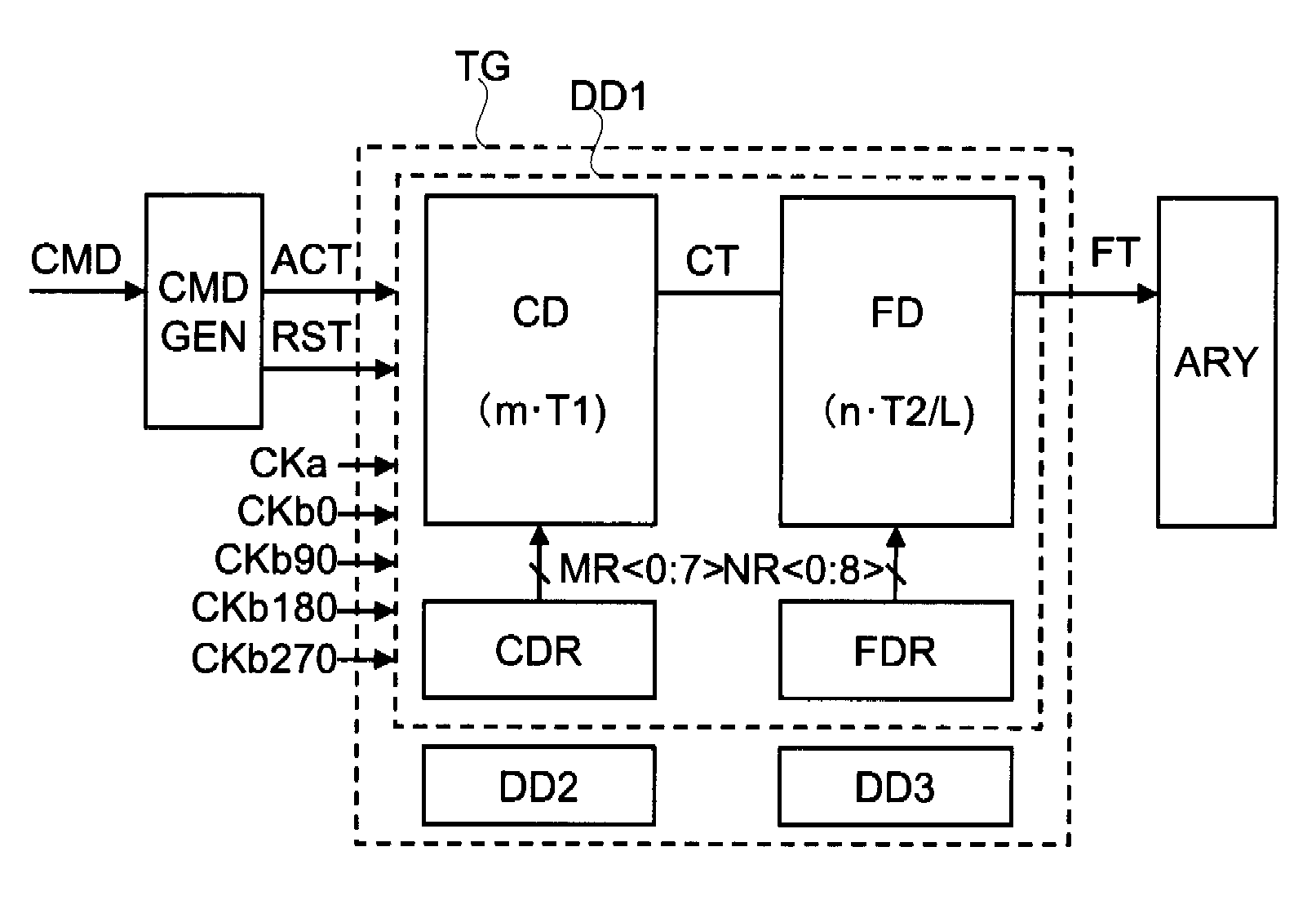
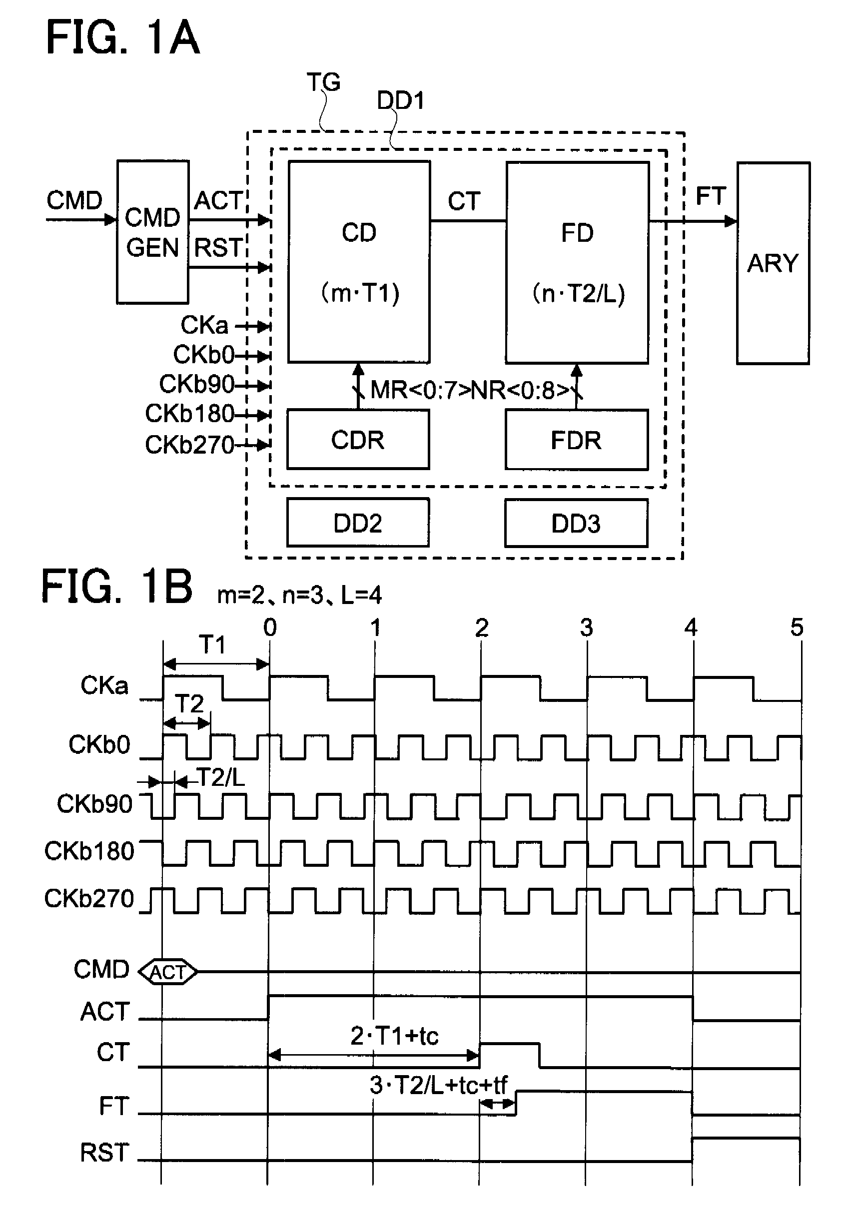
[0064]In the timing control circuit according to the present invention, the inputs are a first clock signal having a first period T1 and a group of second clocks having a second period T2 and constituting clocks of L phases (i.e., L-number of clock signals that differ in phase from each other by approximately T2 / L). When v...


PUM


Abstract

Disclosed is a timing control circuit that receives a first clock having a period T1, a group of second clocks of L different phases spaced apart from each other at substantially equal intervals and selection signals m, n supplied thereto and generates a fine timing signal delayed from the rising edge of the first clock signal by a delay td of approximately td=m·T1+n·(T2 / L). The timing control circuit includes a coarse delay circuit and a fine delay circuit. The coarse delay circuit includes a counter for counting a rising edge of the first clock signal after an activate signal is activated and generates a coarse timing signal whose amount of delay from the first clock signal is approximately m·T1. The fine delay circuit comprises L-number of multiphase clock control delay circuits disposed in parallel, delays by n·T2 / L the timing of sampling of the coarse timing signal by respective clocks of the group of L-phase second clocks, and takes the OR among the resulting delayed pulses to thereby produce the fine timing signal.

Description

REFERENCE TO RELATED APPLICATION[0001]This application is based upon and claims the benefit of the priority of Japanese patent application No. 2007-238013, filed on Sep. 13, 2007, the disclosure of which is incorporated herein in its entirety by reference thereto.FIELD OF THE INVENTION[0002]This invention relates to a timing control circuit. More particularly, the invention relates to a timing control circuit and method suited for timing signal generation in a semiconductor storage device and to a semiconductor storage device having this timing control circuit.BACKGROUND OF THE INVENTION[0003]FIG. 16A is a diagram schematically illustrating a typical configuration of a logic LSI chip. In order to raise the throughput of data processing in a logic LSI chip (LOGIC) in FIG. 16A, a pipeline operation is performed in which the path from a data input (DIN) to a data output (DOUT) is divided into a plurality of logic circuit blocks (LGK) at flip-flops (FF) and the flip-flops (FF1, FF2, and...

Claims


Application Information

Patent Timeline
Patent Type & Authority Patents(United States)
IPC IPC(8): G06F1/04G06F1/06G11C11/407G11C11/4076H03K5/00H03K5/13H03L7/081
CPCG11C7/1072G11C7/222G11C11/4076G11C19/00H03K5/135G11C7/04
Inventor IDE, AKIRATAKAI, YASUHIROSEKIGUCHI, TOMONORITAKEMURA, RIICHIROAKIYAMA, SATORUNAKAYA, HIROAKI
Owner LONGITUDE SEMICON S A R L
Why Eureka
Try Eureka