
Voltage supply circuit, display device, electronic equipment, and voltage supply method

a voltage supply circuit and display device technology, applied in the direction of electric variable regulation, process and machine control, instruments, etc., can solve the problems of increasing the number of manufacturing processes and difficulty in providing greater production volume, and achieve the effect of improving production volume and reducing manufacturing processes and costs

Inactive Publication Date: 2010-08-24
JOLED INC
View PDF11 Cites 7 Cited by
  • Summary
  • Abstract
  • Description
  • Claims
  • Application Information

AI Technical Summary

Benefits of technology

The present invention provides a voltage supply circuit and method that can be incorporated in a panel formed by transistors of identical polarity, resulting in improved production volume and reduced manufacturing processes and cost. The circuit includes first and second nodes and a predetermined potential. An output transistor is connected to the first and second nodes and an active reset signal is used to connect the nodes. The circuit can be adjusted to vary the potentials of the nodes with a predetermined difference maintained therebetween. This allows for a single DC-DC converter to be incorporated in the panel, reducing the number of manufacturing processes required. The invention also provides a display device and electronic equipment with the voltage supply circuit. The technical effects of the invention include improved production volume, reduced manufacturing processes and cost, and improved performance and reliability of the voltage supply circuit.

Problems solved by technology

However, forming a panel with these circuits requires several types of power supplies.
This results in increased number of manufacturing processes, making it difficult to provide greater production volume.

Method used


Image

  • Voltage supply circuit, display device, electronic equipment, and voltage supply method
  • Voltage supply circuit, display device, electronic equipment, and voltage supply method
  • Voltage supply circuit, display device, electronic equipment, and voltage supply method

Examples


first embodiment

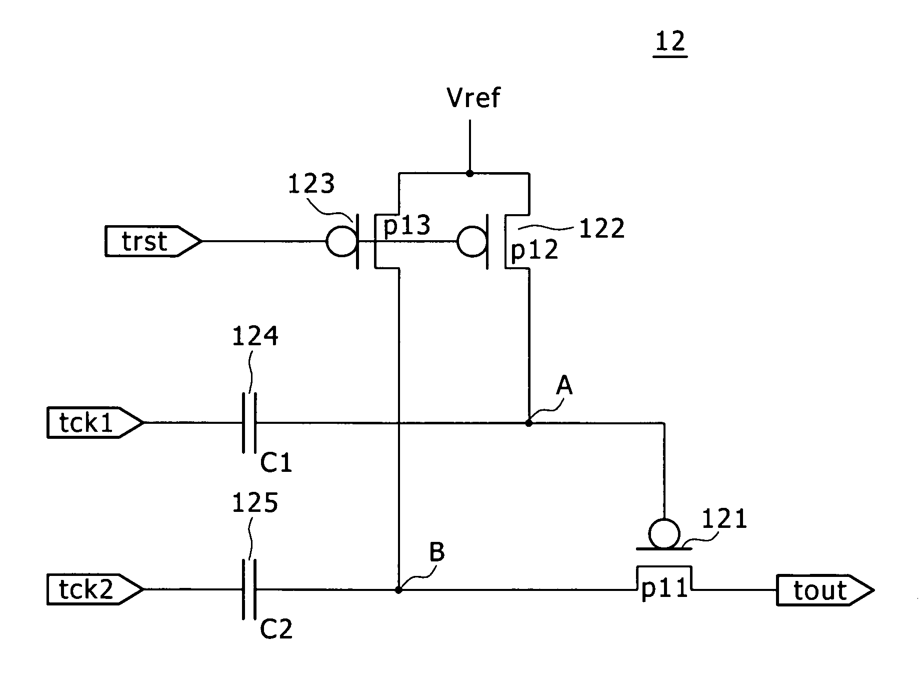
[0079]FIG. 3 is a block diagram illustrating a configuration example of a voltage supply circuit according to a first embodiment of the present invention. FIG. 4 is a circuit diagram illustrating a configuration example of a DC-DC converter according to the first embodiment. FIG. 5 is a timing diagram of the voltage supply circuit according to the first embodiment.

[0080]A voltage supply circuit 10 according to the first embodiment includes an adjustment section 11 and a DC-DC converter (DDcon) 12.

[0081]A denotes a first node, B a second node, ck1 and ck2 first and second clocks which are in phase with each other, and rst a reset signal which is basically reverse in phase to the clocks ck1 and ck2.

[0082]The adjustment section 11 has level shifters (lvlsft) 111, 112 and 113 adapted to adjust the levels of the reset signal rst and the clocks ck1 and ck2.

[0083]The level shifter 111 shifts the amplitude of the reset signal rst to produce a signal having an intermediate amplitude between ...

second embodiment

[0110]FIG. 6 is a block diagram illustrating a configuration example of the voltage supply circuit according to a second embodiment of the present invention. FIG. 7 is a circuit diagram illustrating a configuration example of the DC-DC converter according to the second embodiment. FIG. 8 is a timing diagram of the voltage supply circuit according to the second embodiment.

[0111]A voltage supply circuit 10A according to the second embodiment differs from the voltage supply circuit 10 according to the first embodiment in that a single clock ck is used rather than two clocks. The same circuit 10A further differs from the circuit 10 in that the level shifter 112 of an adjustment section 11A shifts the amplitude of the clock ck as with that of the reset signal rst to produce a signal having an intermediate amplitude between the supply voltage Vdd and the ground potential GND and supplies the signal to a DC-DC converter 12A. The same circuit 10A still further differs from the circuit 10 in...

third embodiment

[0121]FIG. 9 is a block diagram illustrating a configuration example of the voltage supply circuit according to a third embodiment of the present invention.

[0122]A voltage supply circuit 10B according to the third embodiment differs from the voltage supply circuit 10 according to the first embodiment in that, because the reset signal rst is reverse in phase to the first and second clocks ck1 and ck2, and because the first and second clocks ck1 and ck2 are in phase with each other, the single clock ck is used to generate the reset signal rst and the first and second clocks ck1 and ck2 following the amplitude shifting.

[0123]More specifically, a level shifter 111B for the reset signal rst is a level shifter with the inverting function (inverter). The clock ck is fed to three level shifters 111B, 112 and 113 in parallel.

[0124]It should be noted that the inverter 111B can be configured only with transistors of identical polarity, namely, PMOS transistors, as with the DC-DC converter 12.

[...


PUM


Abstract

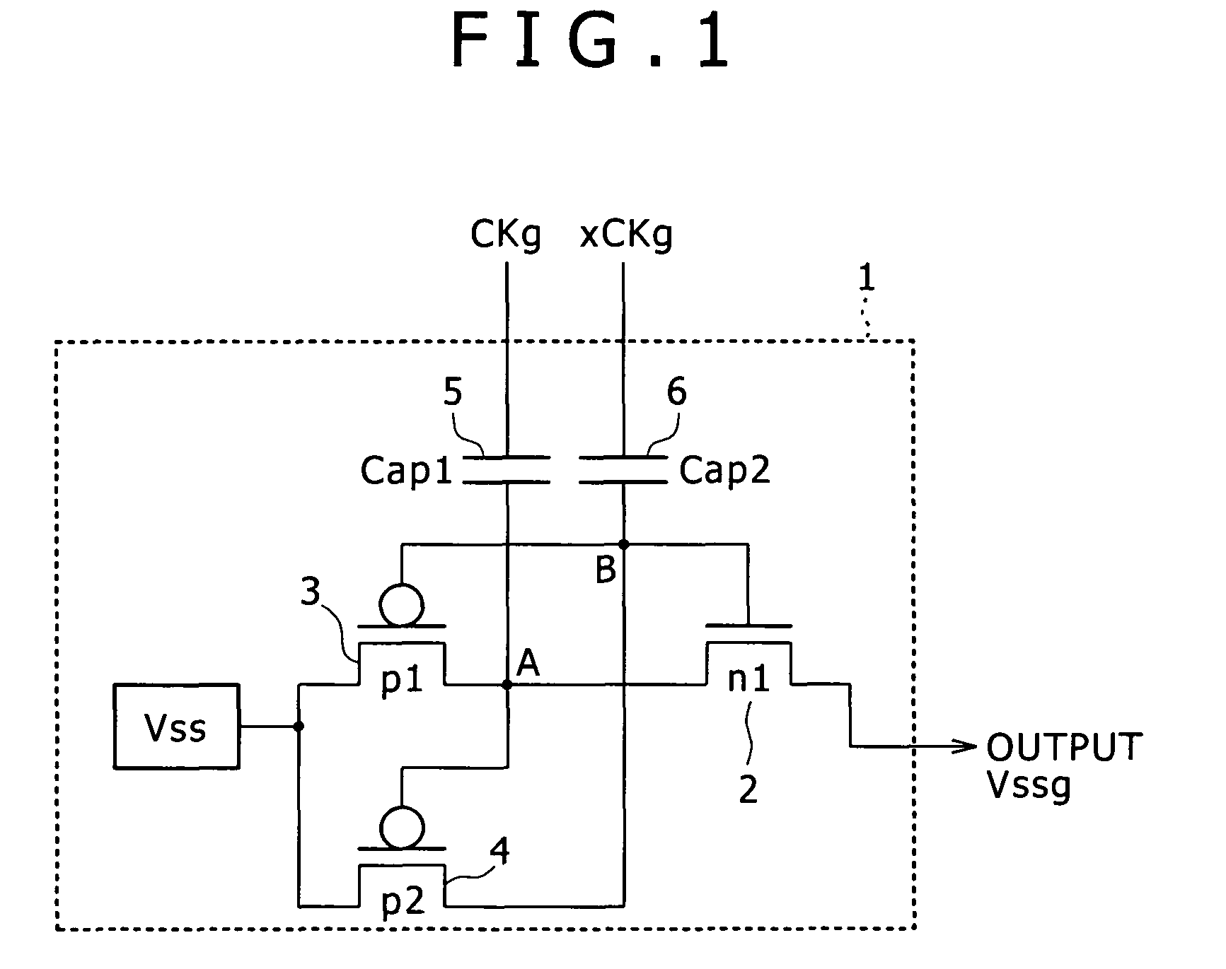
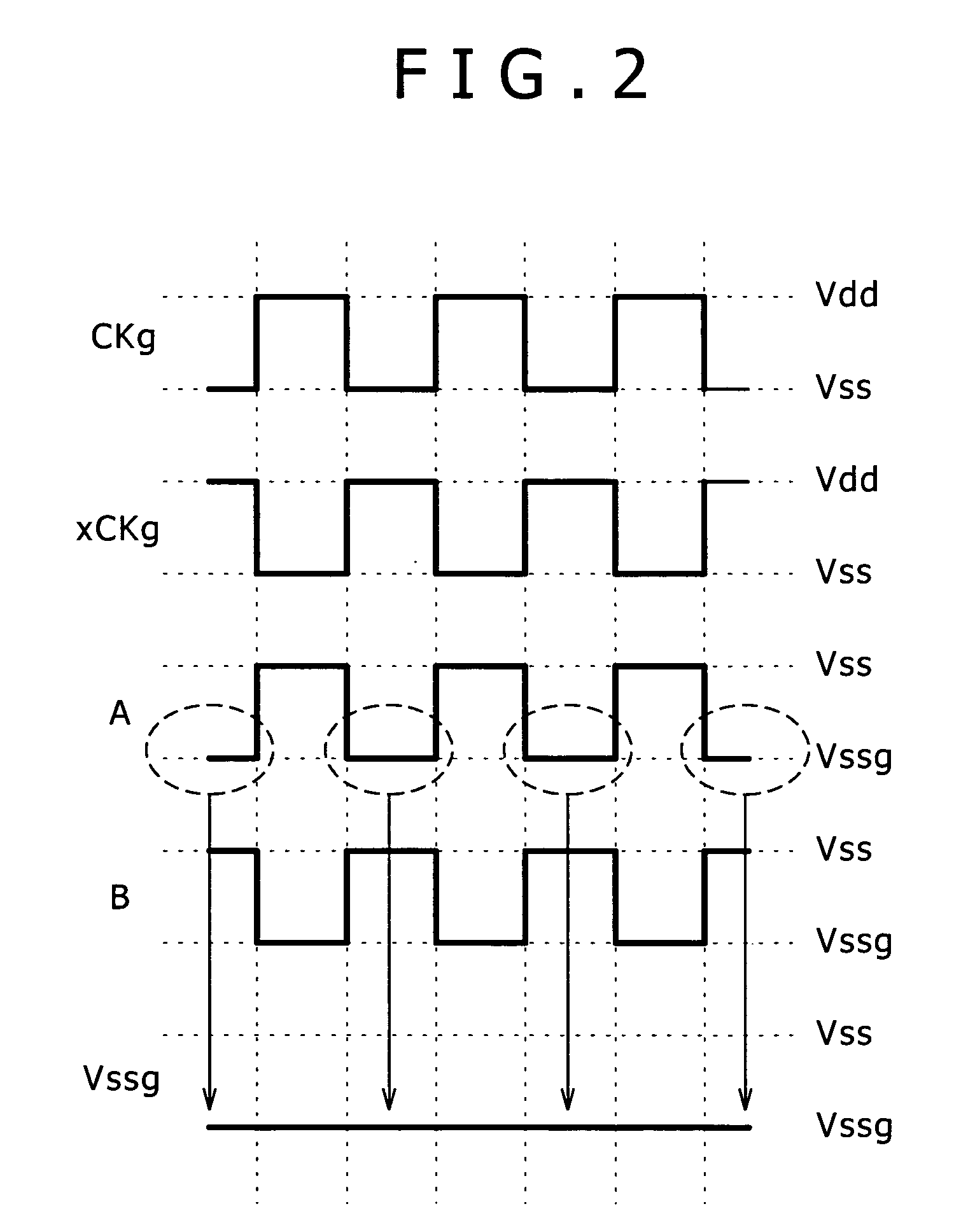
A voltage supply circuit including: first and second nodes; a predetermined potential; and an output transistor having its control terminal connected to the first node, its first terminal connected to the second node and its second terminal connected to an output terminal. The circuit further includes: a switching element which turns on in response to an active reset signal to connect the potential and the first and second nodes together; a first capacitor connected to the first node and supplied with a clock; a second capacitor connected to the second node and supplied with another clock; and an adjustment section adapted to adjust the clock amplitudes so that the potentials of the first and second nodes vary with a predetermined difference maintained therebetween. The reset signal is basically reverse in phase to the clocks.

Description

CROSS REFERENCES TO RELATED APPLICATIONS[0001]The present invention contains subject matter related to Japanese Patent Application JP 2006-355771 filed with the Japan Patent Office on Dec. 28, 2006, the entire contents of which being incorporated herein by reference.BACKGROUND OF THE INVENTION[0002]1. Field of the Invention[0003]The present invention relates to a voltage supply circuit including components such as a DC-DC converter adapted to supply a positive or negative drive voltage to a display device driver. The present invention also relates to a display device and electronic equipment having the same and a voltage supply method using the same.[0004]2. Description of the Related Art[0005]An image display device such as liquid crystal display or organic EL (Electro luminescence) display has a number of pixels arranged in a matrix form. Such a display device displays an image by controlling the optical intensity of each pixel according to image information to be displayed.[0006]...

Claims


Application Information

Patent Timeline
Patent Type & Authority Patents(United States)
IPC IPC(8): G05F1/10H05B44/00
CPCH02M3/07G09G3/20G09G2330/028H03K17/063
Inventor JINTA, SEIICHIRO
Owner JOLED INC
Learn More