
Growth substrates for inverted metamorphic multijunction solar cells

a technology of growth substrates, which is applied in the field of semiconductor devices, can solve the problems of presenting a number of practical difficulties, affecting the production efficiency of solar cells, and requiring a large amount of material and fabrication steps, etc., to achieve commercially established fabrication processes and produce commercially viable and energy efficient inverted metamorphic multijunction solar cells

Active Publication Date: 2010-08-31
SOLAERO TECH CORP
View PDF39 Cites 91 Cited by
  • Summary
  • Abstract
  • Description
  • Claims
  • Application Information

AI Technical Summary

Benefits of technology

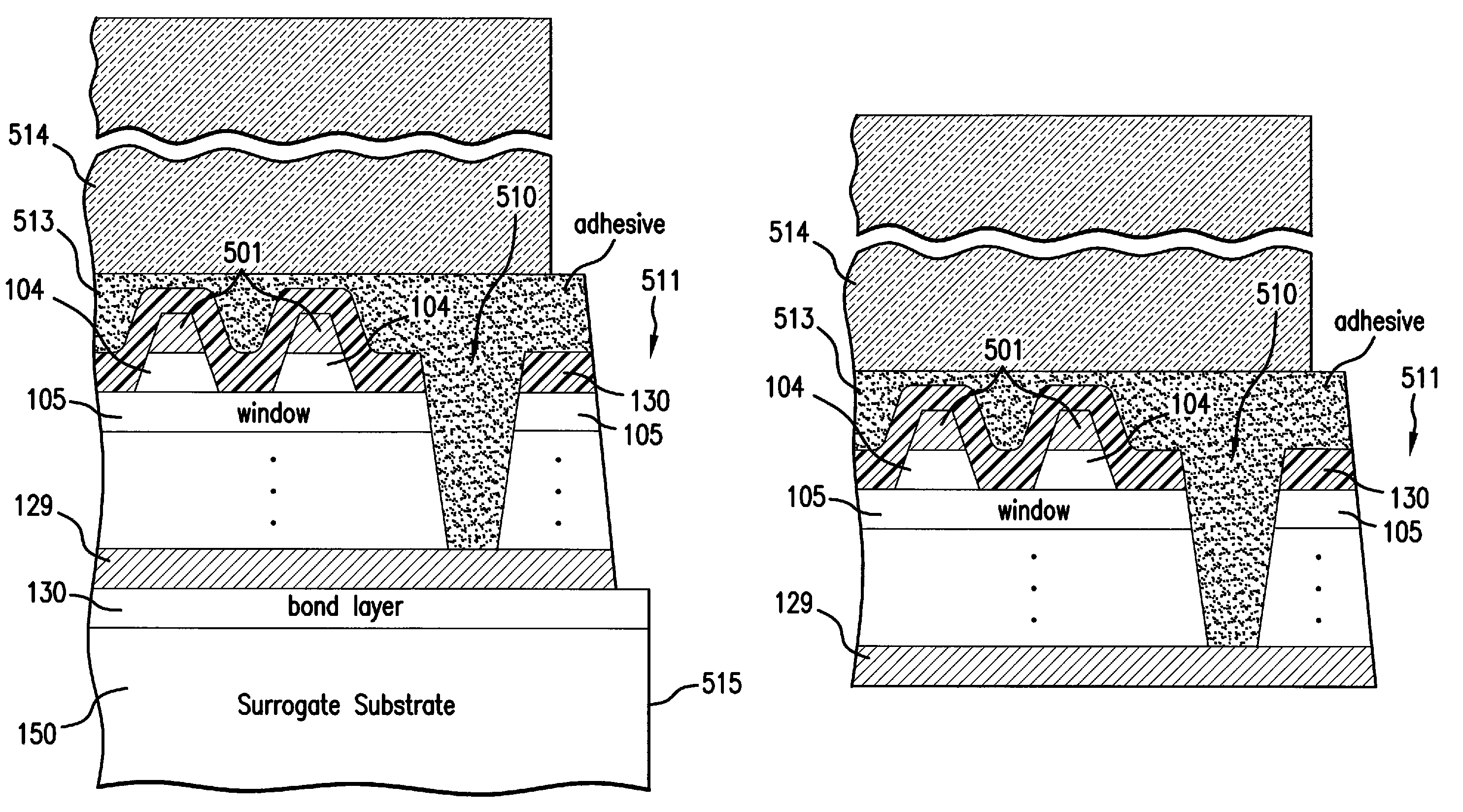
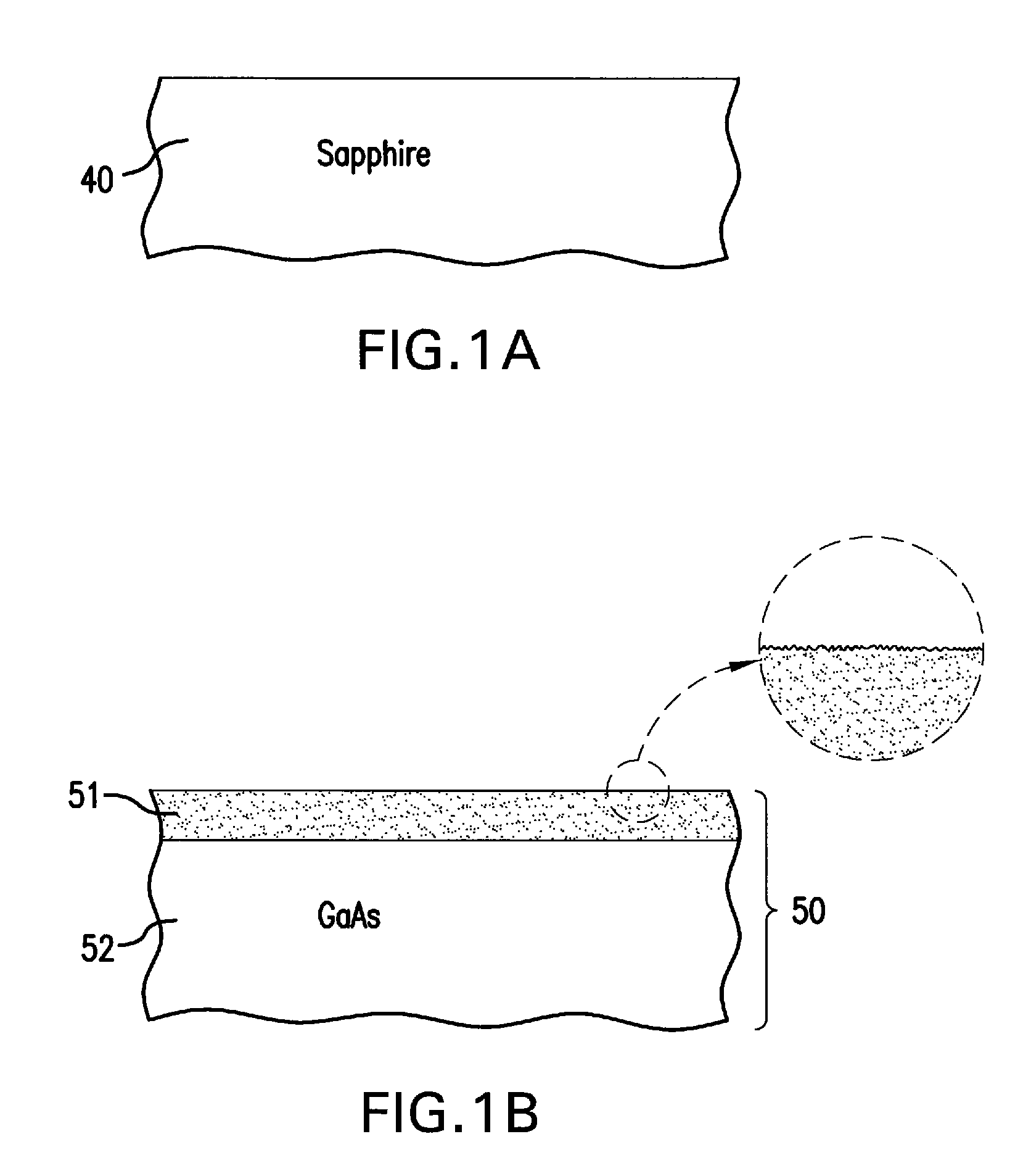
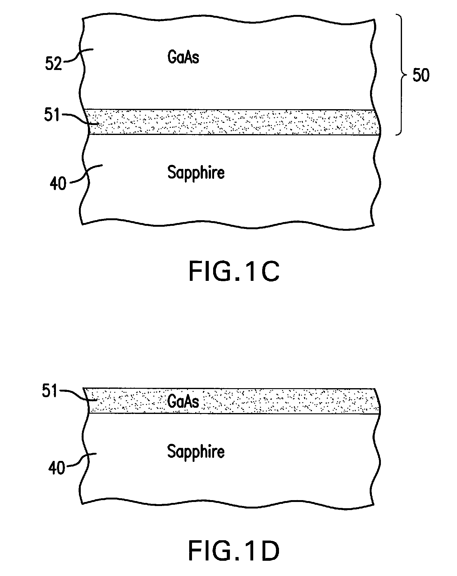
The present invention provides a method of manufacturing a solar cell by bonding a gallium arsenide or germanium carrier to a support substrate, detaching the bulk of the carrier from the composite structure, and depositing a sequence of layers of semiconductor material forming a solar cell on the substrate. The invention also includes forming a new bonding surface on the detached carrier and preparing a new support substrate for bonding to produce a new composite structure. The invention further includes mounting a surrogate second substrate on top of the solar cell and removing the growth substrate. The invention also includes depositing a sequence of layers of semiconductor material forming a solar cell comprising a first subcell, a second subcell, a lattice constant transition material, and a graded interlayer. The invention provides a method for efficiently manufacturing solar cells with improved performance.

Problems solved by technology

Compared to silicon, III-V compound semiconductor multijunction devices have greater energy conversion efficiencies and generally more radiation resistance, although they tend to be more complex to manufacture.
The structures described in such reference present a number of practical difficulties relating to the appropriate choice of materials and fabrication steps, for a number of different layers of the cell.
Prior to the inventions described in this and the related applications noted above, the materials and fabrication steps disclosed in the prior art have not been adequate to produce a commercially viable and energy efficient inverted metamorphic multijunction solar cell using commercially established fabrication processes.

Method used


Image

  • Growth substrates for inverted metamorphic multijunction solar cells
  • Growth substrates for inverted metamorphic multijunction solar cells
  • Growth substrates for inverted metamorphic multijunction solar cells

Examples


Embodiment Construction

[0071]Details of the present invention will now be described including exemplary aspects and embodiments thereof. Referring to the drawings and the following description, like reference numbers are used to identify like or functionally similar elements, and are intended to illustrate major features of exemplary embodiments in a highly simplified diagrammatic manner. Moreover, the drawings are not intended to depict every feature of the actual embodiment nor the relative dimensions of the depicted elements, and are not drawn to scale.

[0072]The basic concept of fabricating an inverted metamorphic multijunction (IMM) solar cell is to grow the subcells of the solar cell on a substrate in a “reverse” sequence. That is, the high band gap subcells (i.e. subcells with band gaps in the range of 1.8 to 2.1 eV), which would normally be the “top” subcells facing the solar radiation, are grown epitaxially on a semiconductor growth substrate, such as for example GaAs or Ge, and such subcells are ...


PUM

PropertyMeasurementUnit
thicknessaaaaaaaaaa
thicknessaaaaaaaaaa
band gapaaaaaaaaaa

Abstract

A method of manufacturing a solar cell by providing a gallium arsenide carrier with a prepared bonding surface; providing a sapphire substrate; bonding the gallium arsenide carrier and the sapphire substrate to produce a composite structure; detaching the bulk of the gallium arsenide carrier from the composite structure, leaving a gallium arsenide growth substrate on the sapphire substrate; and depositing a sequence of layers of semiconductor material forming a solar cell on the growth substrate. For some solar cells, the method further includes mounting a surrogate second substrate on top of the sequence of layers of semiconductor material forming a solar cell; and removing the growth substrate.

Description

REFERENCE TO RELATED APPLICATIONS[0001]This application is related to co-pending U.S. patent application Ser. No. 12 / 271,127 and Ser. No. 12 / 271,192 filed Nov. 14, 2008.[0002]This application is related to co-pending U.S. patent application Ser. No. 12 / 267,812 filed Nov. 10, 2008.[0003]This application is related to co-pending U.S. patent application Ser. No. 12 / 258,190 filed Oct. 24, 2008.[0004]This application is related to co-pending U.S. patent application Ser. No. 12 / 253,051 filed Oct. 16, 2008.[0005]This application is related to co-pending U.S. patent application Ser. No. 12 / 190,449 filed Aug. 12, 2008.[0006]This application is related to co-pending U.S. patent application Ser. No. 12 / 187,477 filed Aug. 7, 2008.[0007]This application is related to co-pending U.S. patent application Ser. No. 12 / 218,558 and U.S. patent application Ser. No. 12 / 218,582 filed Jul. 16, 2008.[0008]This application is related to co-pending U.S. patent application Ser. No. 12 / 123,864 filed May 20, 200...

Claims


Application Information

Patent Timeline
Patent Type & Authority Patents(United States)
IPC IPC(8): H01L21/30H01L21/46
CPCH01L29/045H01L31/0392H01L31/06875H01L31/0735H01L31/078H01L31/1844H01L31/1892H01L31/1852Y02E10/544Y10S438/977Y02P70/50
Inventor SHARPS, PAUL R.CORNFELD, ARTHURVARGHESE, TANSENNEWMAN, FREDDIAZ, JACQUELINE
Owner SOLAERO TECH CORP
Learn More