Photomask and manufacturing method of semiconductor device

a manufacturing method and semiconductor technology, applied in the field of photomasks and semiconductor device manufacturing methods, can solve the problems of difficulty in forming fine patterns and fine pitches, depth of focus, phase edge technique of forming such fine patterns has a problem, etc., and achieves high reliability and uniform line widths. , the effect of high-quality semiconductor devices

Inactive Publication Date: 2010-09-07
FUJITSU SEMICON LTD
View PDF18 Cites 6 Cited by
  • Summary
  • Abstract
  • Description
  • Claims
  • Application Information

AI Technical Summary

Benefits of technology

[0009]The present invention is made in view of the aforementioned problem, and its object is to provide a photomask and a manufacturing method of a semiconductor device which make it possible to manufacture a highly reliable semiconductor device by improving a common depth of focus of patterns to thereby realize highly uniform line widths when the patterns are transferred by a double exposure process.

Problems solved by technology

In recent years, with the scaling down of a device, it becomes difficult to form a fine pattern and a fine pitch, and hence a double exposure process in which two photomasks are used in one layer is introduced to form the fine pattern.
However, the phase edge technique of forming such fine patterns has a problem.
The problem is a depth of focus.
Moreover, also in gate electrode patterns formed by the double exposure process, it is similarly difficult to obtain a sufficient depth of focus when the photomask to form the normal patterns is exposed.

Method used


Image

  • Photomask and manufacturing method of semiconductor device
  • Photomask and manufacturing method of semiconductor device
  • Photomask and manufacturing method of semiconductor device

Examples


first embodiment

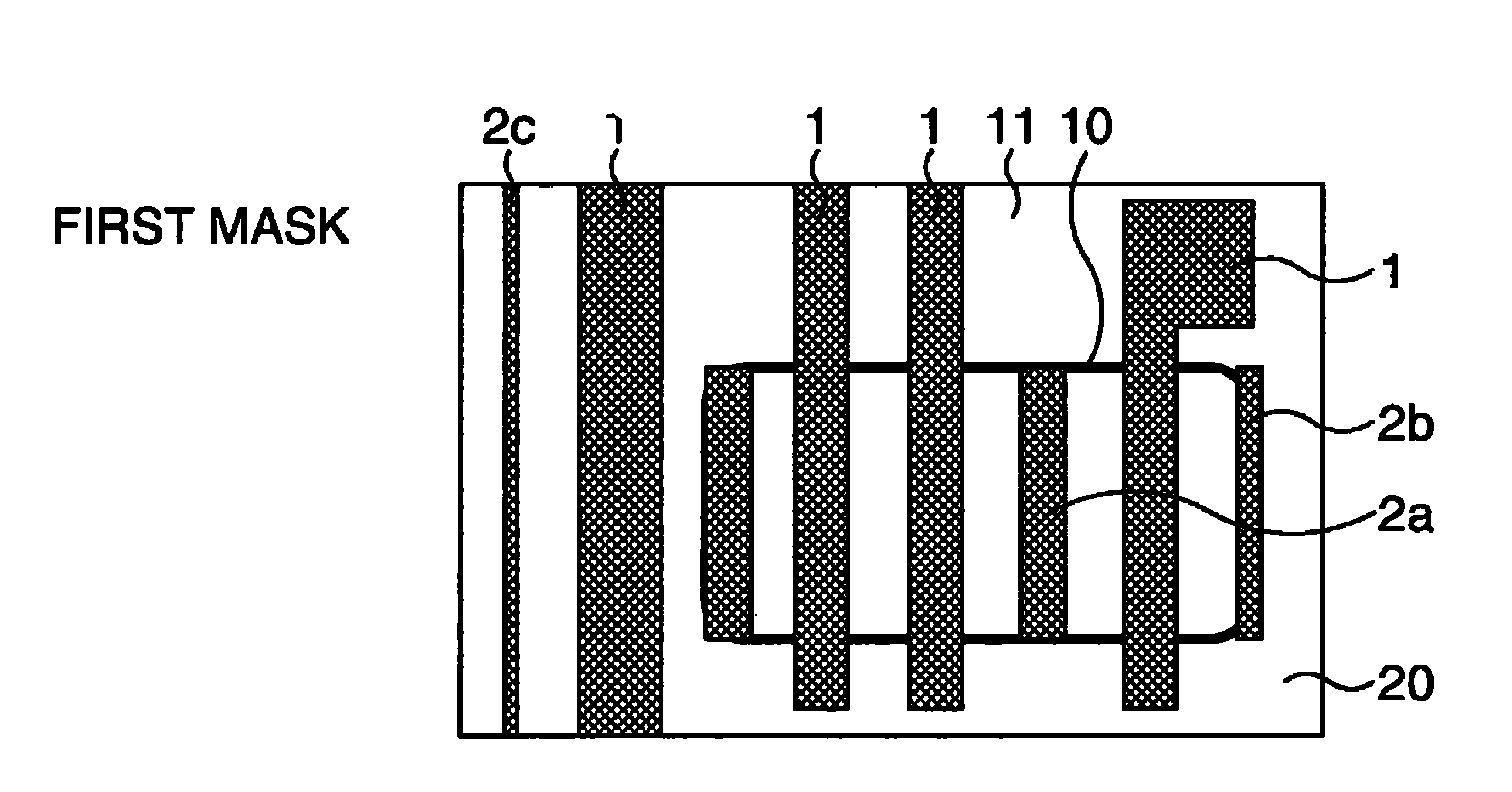
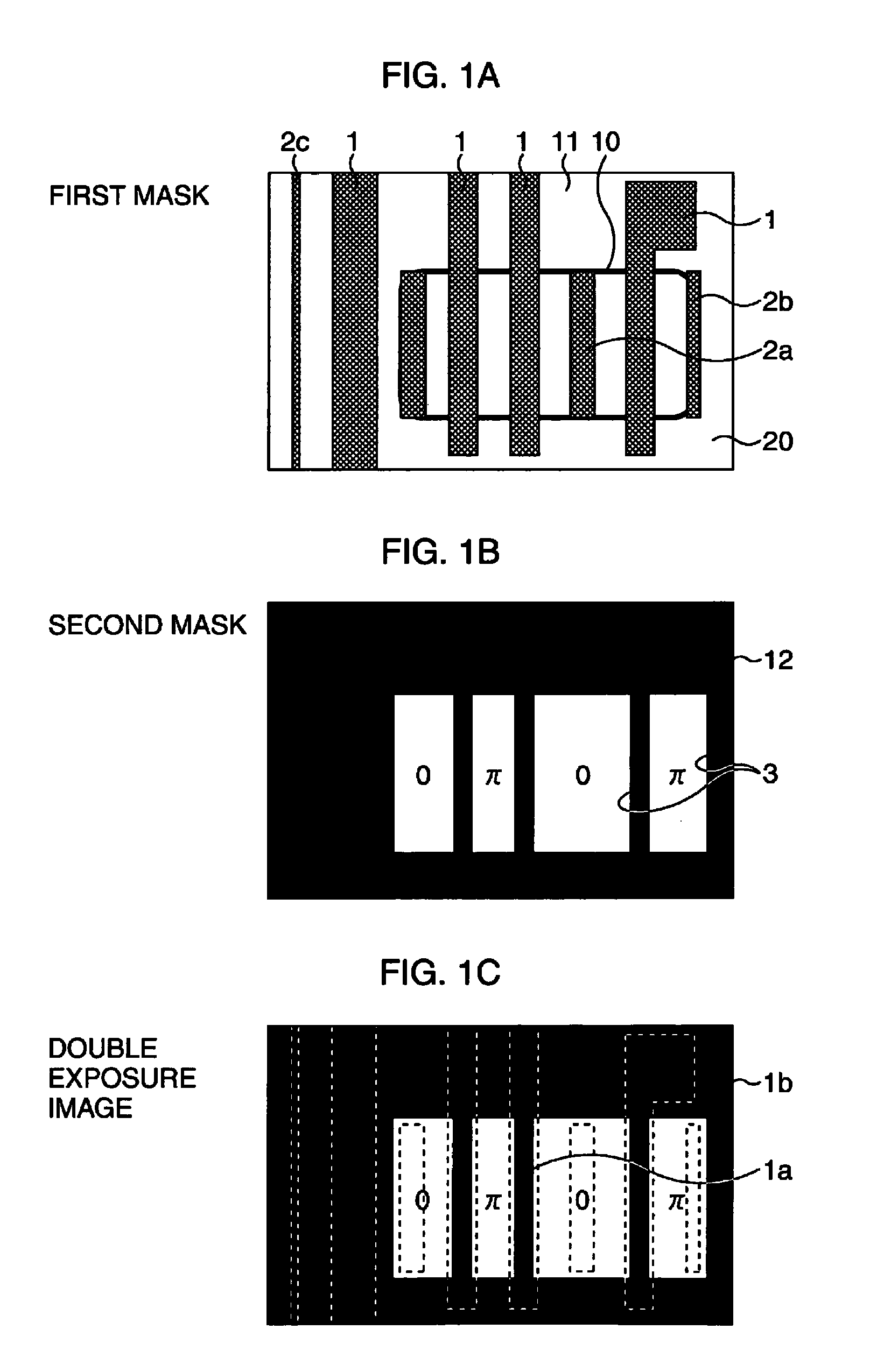
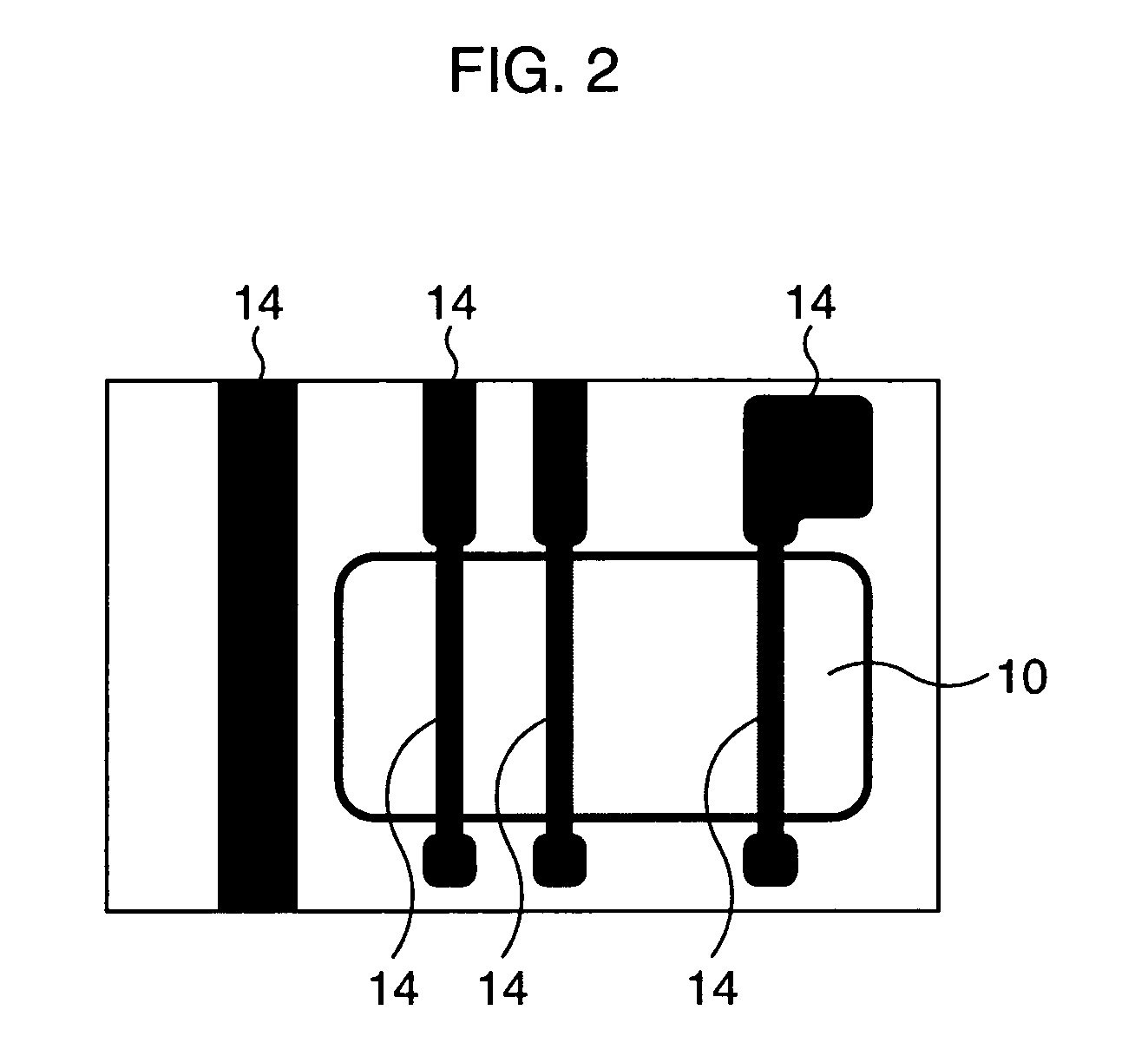
[0028]FIG. 1A to FIG. 1C are schematic plan views for explaining a manufacturing method of a semiconductor device including a gate according to the first embodiment. Here, an explanation will be given with a particular emphasis on a process of forming gate patterns by a phase edge technique.

[0029]A first photomask 11 is a halftone phase shift mask (for example, a transmittance of 6%) for an ArF excimer laser as shown in FIG. 1A. This photomask 11 includes gate patterns 1 to form gates and assist patterns 2a, 2b, and 2c to be inserted into portions in each of which a distance between the gate patterns 1 is large. Here, the assist pattern 2a has a shape corresponding to only a position of an active region 10 to be exposed, the assist pattern 2b is formed to have a resoluble line width, which is different from the assist pattern 2a, and these assist patterns 2a and 2b have each a line width optimized according to the line widths of and space width between the respective gate patterns 1...

second embodiment

[0043]FIG. 4A to FIG. 4C are schematic plan views for explaining a manufacturing method of a semiconductor device including a gate according to the second embodiment. Here, an explanation will be given with a particular emphasis on a process of forming gate patterns by the phase edge technique.

[0044]A first photomask 21 is a halftone phase shift mask (for example, a transmittance of 6%) for an ArF excimer laser as shown in FIG. 4A. This photomask 21 includes gate patterns 1 to form gates and assist patterns 23 each having a line width equal to or smaller than a resolution limit which are to be inserted into portions in each of which a distance between the gate patterns 1 is large. Here, all the assist patterns 23 have the same width, for example, from approximately 50 nm to approximately 60 nm on the wafer substrate 20.

[0045]A second photomask 22 is a Levenson phase shift mask for the ArF excimer laser as shown in FIG. 4B. The photomask 22 includes shifter patterns 3 corresponding t...

third embodiment

[0051]FIG. 5A to FIG. 5C are schematic plan views for explaining a manufacturing method of a semiconductor device including a gate according to the third embodiment. Here, an explanation will be given with a particular emphasis on a process of forming gate patterns by the phase edge technique.

[0052]A first photomask 31 is a halftone phase shift mask (for example, a transmittance of 6%) for an ArF excimer laser as shown in FIG. 5A. This photomask 31 includes gate patterns 1 to form gates and assist patterns 24a, 24b, and 24c to be inserted into portions in each of which a distance between the gate patterns 1 is large. Here, a narrow-width portion of the assist pattern 24a is formed to have a line width equal to or smaller than a resolution limit, a wide-width portion thereof is formed to have a resoluble line width, the assist pattern 24b is formed to have a resoluble line width which is different from the assist pattern 24a, and these assist patterns 24a and 24b respectively have li...


PUM

PropertyMeasurementUnit
transmittanceaaaaaaaaaa
thicknessaaaaaaaaaa
thicknessaaaaaaaaaa

Abstract

A double exposure process is performed using a halftone phase shift mask (11) including gate patterns (1), assist patterns (2a) and (2b) with different resoluble line widths, and an assist pattern (2c) with a line width equal to or smaller than a resolution limit which are respectively inserted into portions in each of which a distance between the gate patterns (1) is large, and a Levenson phase shift mask (11) including shifter patterns (3) corresponding to the gate patterns (1) of the photomask 11. On this occasion, the assist patterns (2a), (2b), and (2c) are erased and only the gate patterns (1) are transferred. Consequently, when patterns are transferred by the double exposure process, a common depth of focus of the patterns is improved and highly uniform line widths are realized, which makes it possible to manufacture a highly reliable semiconductor device.

Description

[0001]This application is a continuation of international application PCT / JP03 / 02211 filed on Feb. 27, 2003.TECHNICAL FIELD[0002]The present invention relates to a photomask and a manufacturing method of a semiconductor device, and particularly it is suitable for application to a case where an extremely fine-sized gate is formed.BACKGROUND ART[0003]In recent years, with the scaling down of a device, it becomes difficult to form a fine pattern and a fine pitch, and hence a double exposure process in which two photomasks are used in one layer is introduced to form the fine pattern. At present, in the double exposure process, a phase edge technique attracts the greatest attention. This technique is mainly used for gate formation, and in a region where a fine gate pattern is formed, a Levenson phase shift mask is used in addition to a photomask (binary mask or halftone phase shift mask) to form a normal pattern. The Levenson phase shift mask has the effect of, by arranging 0 / π phase shi...

Claims


Application Information

Patent Timeline
Patent Type & Authority Patents(United States)
IPC IPC(8): G03F9/00G03F7/26G03F1/30G03F1/32G03F1/68G03F7/00G03F7/20H01L21/027H01L21/28H01L29/423H01L29/49
CPCG03F1/144G03F7/203G03F1/0061G03F1/30G03F1/32G03F1/36G03F1/70
Inventor MINAMI, TAKAYOSHI
Owner FUJITSU SEMICON LTD
Why Eureka
Try Eureka