Pattern formation method, electronic circuit manufactured by the same, and electronic device using the same

a technology of electronic circuits and patterns, applied in the field of methods for forming patterns and electronic circuits, can solve the problems of high environmental burden, high production cost, and high production cost, and achieve the effects of reducing the number of steps, reducing the cost and environmental burden, and improving throughpu

Inactive Publication Date: 2010-09-07
ASAHI GLASS CO LTD
View PDF42 Cites 1 Cited by
  • Summary
  • Abstract
  • Description
  • Claims
  • Application Information

AI Technical Summary

Benefits of technology

[0044]The pattern forming method according to the present invention can reduce the cost and the environmental burden since the opening forming step is performed under a dry condition as explained. Heretofore, exposure, development and the like have been performed under a wet condition in order to form an opening. However, the pattern forming method according to present invention can form an opening without exposure or development and can significantly reduce the number of the steps since the method is performed under a dry condition. For example, when the method uses a material that can be patterned by being directly removed under a dry condition, direct patterning by a laser beam can be combined to form a pattern more effectively. As a result, the throughput is improved by a significant reduction in the number of the steps, and the facility investment and the cost for indirect materials, such as a chemical liquid, can be significantly reduced by the improved throughput. Accordingly, the present invention has an advantage of being capable of forming a pattern at low cost by a significant reduction in manufacturing cost. Further, it is expected to remarkably improve the yield since it is possible to significantly reduce the number of the steps.
[0045]Heretofore, a chemical liquid, such as a developer or a cleaning agent, has been used to perform exposure, development and the like under a wet condition. However, the method according to the present invention is performed under a dry condition without using such a chemical liquid. Accordingly, the present invention is also applicable to a material that has been difficult to form a pattern under a conventional wet condition. Further, the present invention also has advantages of being capable of not only avoiding the generation of liquid waste caused by use of a chemical liquid but also performing the method with low environmental burden.
[0046]The present invention also has an advantage of improving reliability since it is possible to restrain an edge portion of a pattern from being exposed, which has been difficult to be done by conventional etching.
[0047]In the above-mentioned pattern forming method, the above-mentioned opening can be formed by a single step since the above-mentioned opening is formed by irradiating the first laser beam to the mask layer. As a result, the present invention has an advantage of being capable of significantly reducing the number of the steps.
[0048]The above-mentioned pattern forming method can further reduce the cost and the environmental burden since the removing step is performed under a dry condition. Although heretofore, a chemical liquid has been used even to remove a mask layer, the present invention does not need to use a chemical liquid since the method is performed under a dry condition. Accordingly, the present invention has an advantage of being capable of performing the method at lower cost and with lower environmental burden.
[0049]The above-mentioned pattern forming method has an advantage of being capable of more easily removing the mask layer since the adhesive force reducing step is contained to reduce the adhesive force between the substrate and the mask layer before the removing step. Further, the above-mentioned pattern forming method can easily reduce the adhesive force since light is irradiated to the mask layer or the mask layer is heated in the adhesive force reducing step. In other words, the present invention has advantages of being capable of not only reducing the adhesive force by a simpler way but also performing the removal more easily.

Problems solved by technology

For this reason, this method has caused a problem in that the production cost is quite high.
Further, this method needs to use a large amount of developer, a chemical liquid, such as an etching agent, and a cleaning liquid when such many processes are performed.
This has caused problems in that not only the production cost is quite high because of low yield but also the environmental burden, such as liquid waste disposal, which has been recently a matter of serious concern, is quite high.
However, the above-mentioned method using a metal mask has caused a problem in that since a metal mask lifts from a substrate to make a minute gap between the substrate and the metal mask, a material for a circuit pattern soaks into the gap on deposition of a thin film, causing a limitation to improvement in the formation precision of a pattern.
Since the adhesion of the metal mask to the substrate is not good, this problem is significant particularly when forming a long continuous pattern.

Method used


Image

  • Pattern formation method, electronic circuit manufactured by the same, and electronic device using the same
  • Pattern formation method, electronic circuit manufactured by the same, and electronic device using the same
  • Pattern formation method, electronic circuit manufactured by the same, and electronic device using the same

Examples


example 1

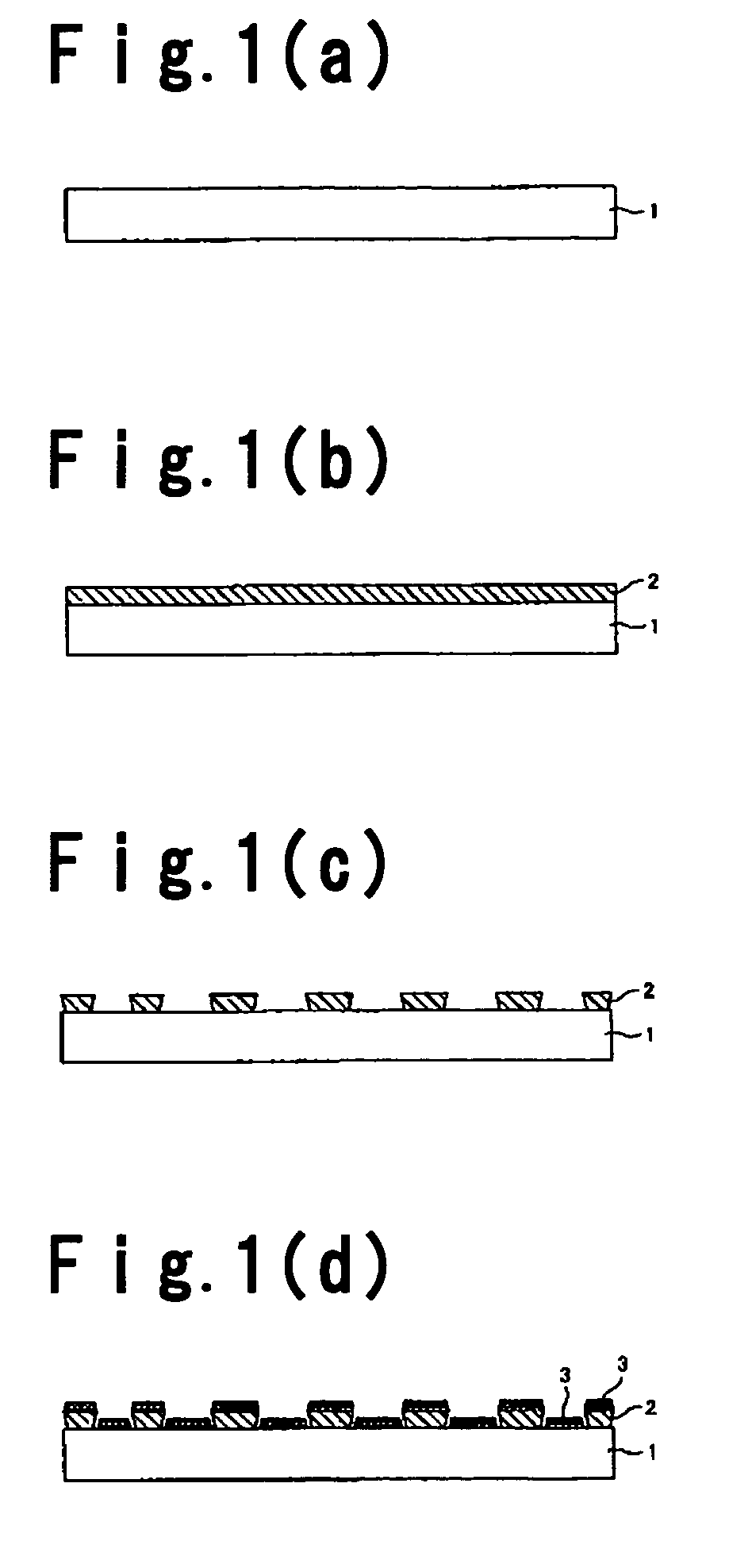
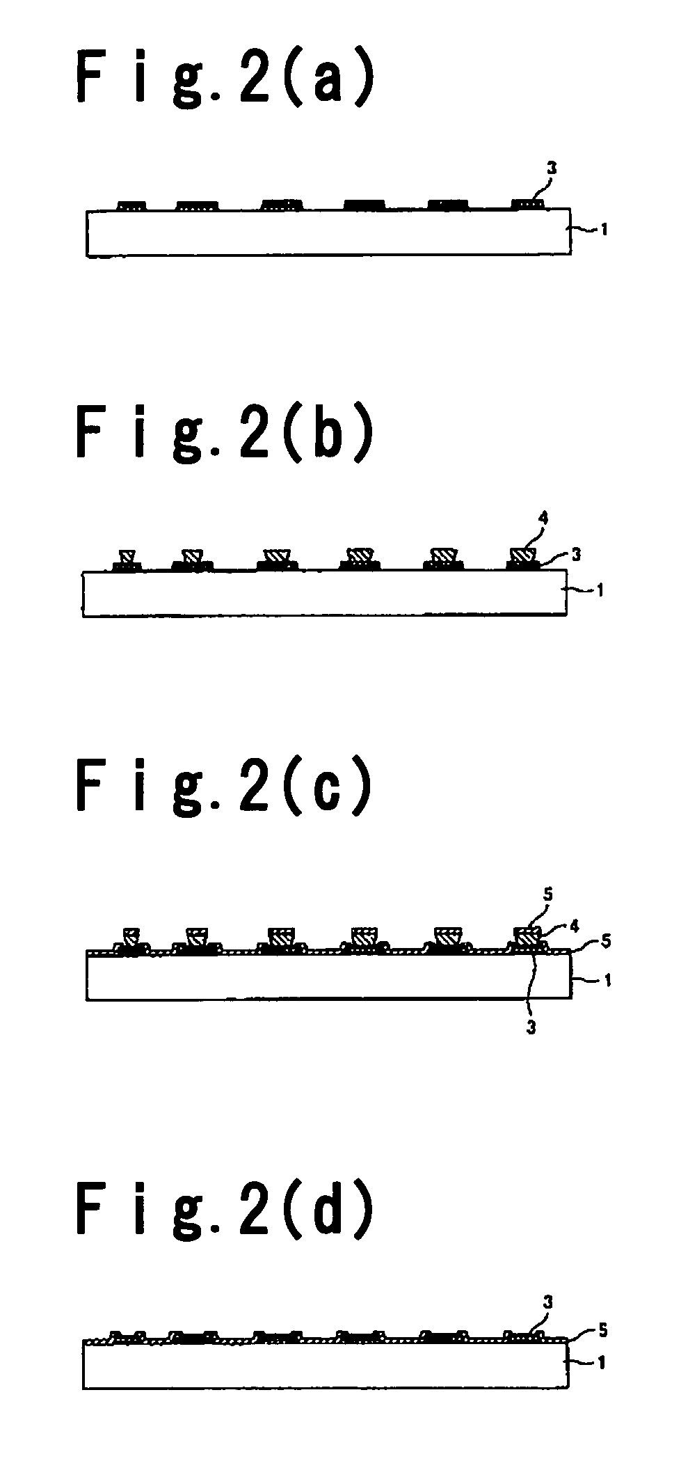
[0158]In this example, explanation will be made, based on FIG. 6 through FIG. 10, about a case which is suited for a process for using a thin film to form electrodes and wires in order to fabricate a high density of electronic circuit module with LSI (Large-Scale Integration) circuits mounted in a high density thereon. FIG. 6 is a cross-sectional view showing a portion of a thin film circuit pattern with two LSI circuits mounted thereon. As shown in FIG. 6, a glass substrate 6 has electrodes 9 and a wiring pattern 10 formed thereon, the electrodes being connected, through a coupling agent 8, to LSI circuits 7 having twelve terminals, and the wiring pattern making connection between the electrodes 9. FIG. 7 is a plan view partly showing the electrodes 9 and the wiring pattern 10 before mounting of the two LSI circuits 7. FIG. 6 is a cross-sectional view taken along the line A-A′ of FIG. 7, looking in the direction of the arrows. FIG. 8 is a plan view showing a state wherein the wirin...

example 2

[0163]Now, the pattern forming method according to a second example will be described, based on FIG. 11 through FIG. 14, about a plasma display (hereinbelow, referred to as “PDP”), which is a typical flat panel display. FIG. 11 shows a representative electrode wiring pattern, which is formed on a surface of a glass substrate 20 as the screen side of a PDP. FIG. 12 is an enlarged view of a portion encircled by the dotted circle 21 in FIG. 11. The electrodes have a typical structure wherein transparent electrodes 22 made of ITO, SnO2 or the like are integrally combined with bus electrodes 23 made of a combination of Cr / Cu / Cr, Cr / Al / Cr or the like and serving as power feeding lines, forming many linear patterns so as to correspond to the number of pixels. In the electrode wiring pattern in this example shown in FIG. 13 and FIG. 14, a pair of a transparent electrode layer 22 and a bus electrode layer 23 is formed, and each of the layers may be fabricated by substantially the same proces...

example 3

[0169]The pattern forming method according to another example will be described, based on FIG. 9 through FIG. 14, about a PDP as a typical flat panel display.

[0170]FIG. 11 is a plan view showing a schematic structure of a thin film circuit pattern (electrode wiring pattern), which is formed on a surface of a glass substrate 20 as the screen side of a PDP. FIG. 12 is a plan view of a portion encircled by the dotted circle 21 in FIG. 11.

[0171]The electrode wiring pattern of this example is configured so that a pair of a transparent electrode layer 22 and a bus electrode layer 23 is formed as shown in FIG. 13 or FIG. 14 (each being a cross-sectional view showing a schematic structure of a thin film circuit pattern in Example 3), more specifically, transparent electrodes (thin-film layer) 22 made of ITO are integrally combined with bus electrodes (thin-film layer) 23 made of a combination of Cr / Cu / Cr and serving as power feeding lines, forming many linear patterns so as to correspond to...


PUM


Abstract

There is provided a method for forming a continuous thin film circuit pattern with good precision, at low cost and with low environmental burden; an electronic circuit fabricated by the same, and an electronic device including the same.There are a step for forming a mask layer 2 on a substrate 1; a step for forming an opening pattern in the mask layer 2; a step for forming a thin film 3 on the substrate 1 and on the mask layer 2; and a step for removing, from the substrate 1, the mask layer 2 and a portion of the thin film 3 formed on the mask layer 2; wherein the opening pattern is formed under a dry condition.

Description

FIELD OF THE INVENTION[0001]The present invention relates to a method for forming a pattern, an electronic circuit fabricated by the same, and an electronic device using the same, such as PDP. More specifically, the present invention relates to a method for forming a circuit pattern comprising a thin film, which is applicable to, e.g., semiconductor integrated circuits or electronic circuits, an electronic circuit fabricated by the same, and any kind of electronic device using a circuit pattern comprising a thin film, which is applicable to, e.g., semiconductor devices, various kinds of computers or various kinds of display devices.DISCUSSION OF BACKGROUND[0002]Heretofore, all kinds of electronic devices, which are applied to computers, communication, information appliances, various kinds of display devices or the like, have used a circuit pattern, which comprises a thin film formed on a substrate and made of metal or an insulating material. In order to copy with the advanced inform...

Claims


Application Information

Patent Timeline
Patent Type & Authority Patents(United States)
IPC IPC(8): H01L21/00H01L21/027H01L21/768
CPCH01L21/0272H01L21/76838
Inventor SATOH, RYOHEIIWATA, YOSHINORINAKAGAWA, KOJIUSUI, REO
Owner ASAHI GLASS CO LTD
Why Eureka
Try Eureka