Semiconductor device

a technology of semiconductors and devices, applied in the field of integrated circuits, can solve the problems of limited application area of transistors, limited enhancement efficiency of devices, and limited increase of driving current by single strain layer, so as to enhance device efficiency, increase driving current, and effectively increase local mechanical stress

Active Publication Date: 2010-09-21
UNITED MICROELECTRONICS CORP
View PDF8 Cites 2 Cited by
  • Summary
  • Abstract
  • Description
  • Claims
  • Application Information

AI Technical Summary

Benefits of technology

[0008]The present invention is to provide a semiconductor device and a fabrication method thereof, wherein the local mechanical stress is effectively increased to raise the driving current and to enhance of the efficiency of the device.
[0051]In accordance to the fabrication method of the invention, asides form fabricating a strain layer at the periphery of the transistor, a strain auxiliary layer is also formed to enhance the stress being provided by the strain layer. Hence, the local mechanical stress is effectively increased to raise the driving current and to enhance to efficiency of the device.
[0052]Moreover, in accordance to the invention, the local mechanical stress can be effectively increased without complicating the fabrication process.

Problems solved by technology

However, limited by the mobility of electrons and holes in the silicon channel, the area of application of a transistor is limited.
However, the increase of the driving current by a single strain layer is very limited.
Hence, to enhance the efficiency of the device becomes restricted.

Method used


Image

  • Semiconductor device
  • Semiconductor device
  • Semiconductor device

Examples


Embodiment Construction

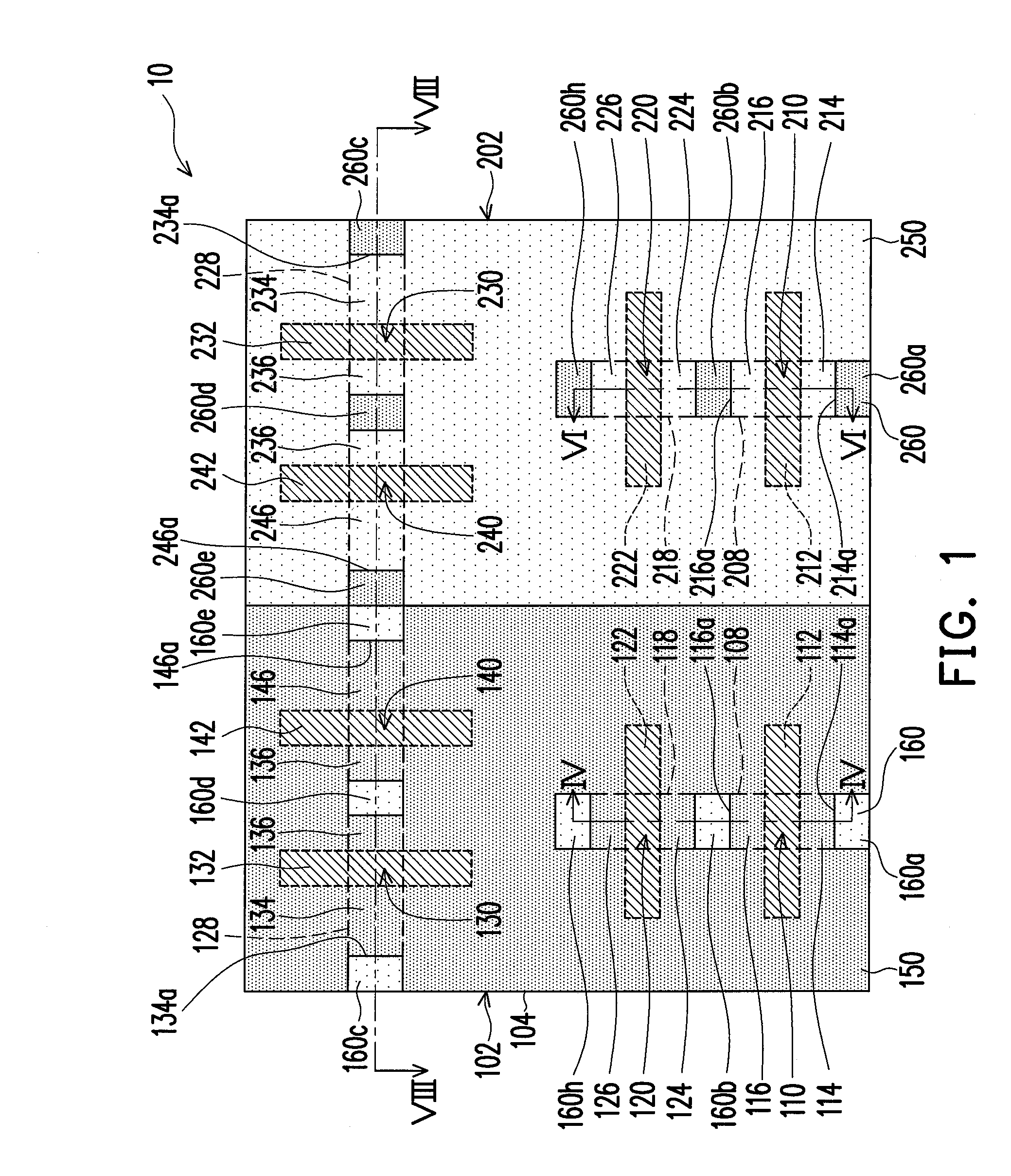
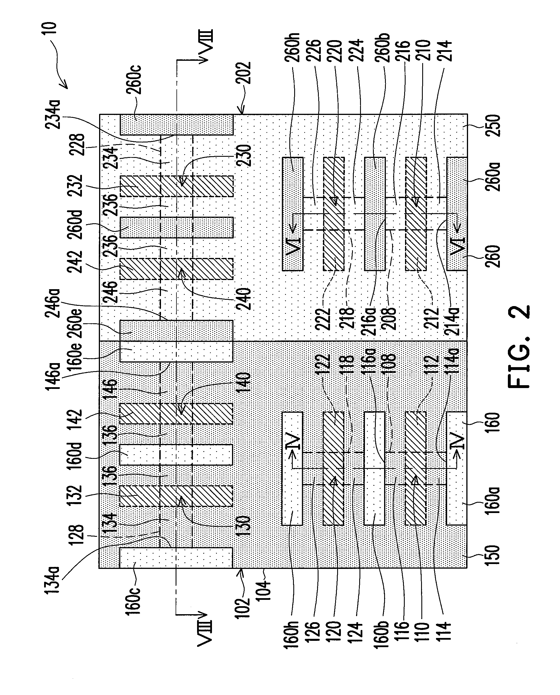
[0062]FIG. 1 is a schematic, upper-view, diagram of a semiconductor device according to one embodiment of the invention. FIG. 2 is a schematic, top-view diagram of a semiconductor device according to another embodiment of the present invention. FIG. 3 is a schematic, top-view diagram of a semiconductor device according to yet another embodiment of the present invention.

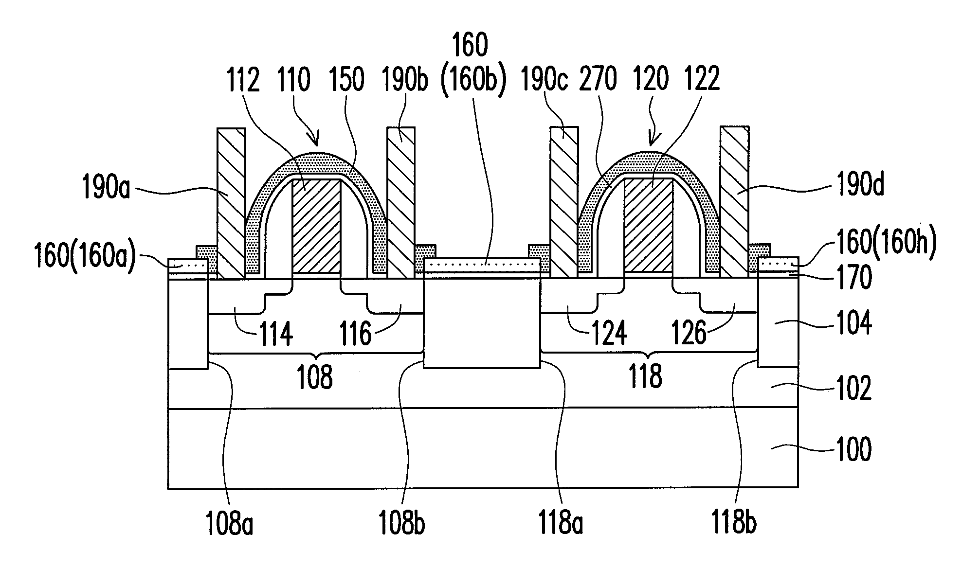
[0063]Referring to FIG. 1 or 2, a semiconductor device 10 of the present invention is formed on the substrate 100. The substrate 100 is, for example, a semiconductor substrate, such as a silicon substrate. The silicon substrate includes n-type dopants or p-type dopants therein. The n-type dopants include but not limited to phosphorous or arsenic. The p-type dopants include boron, for example. The substrate 100 may also be silicon-on-isolator (SOI), which includes an insulation layer having a silicon substrate thereover. The substrate includes an n-type well region 102 and a p-type well region 202. The n-type well regi...


PUM


Abstract

A semiconductor is provided. The semiconductor device includes a transistor, a first strain layer and a second strain layer on a substrate. The first strain layer is configured at the periphery of the transistor. The second strain layer covers the transistor and a region exposed by the first strain layer. The stress provided by the second strain layer is different from that by the first strain layer.

Description

BACKGROUND OF THE INVENTION[0001]1. Field of Invention[0002]The present invention relates to an integrated circuit and a method of fabricating the same; more particularly, the present invention relates to a semiconductor device and a method of fabricating the same.[0003]2. Description of Related Art[0004]With the development of technology in electronic equipments for communication, etc., the operating speed of a transistor increases rapidly. However, limited by the mobility of electrons and holes in the silicon channel, the area of application of a transistor is limited.[0005]Altering the mobility of electrons and holes in the channel by controlling the mechanical stress in the channel is one approach to enhance the operational speed of a transistor.[0006]Conventionally, the silicon germanium (SiGe) type of material has been proposed for forming the source / drain regions of the transistor, wherein portions of the substrate designated for forming the source / drain regions are removed. ...

Claims


Application Information

Patent Timeline
Patent Type & Authority Patents(United States)
IPC IPC(8): H01L27/108
CPCH01L21/823412H01L21/823807H01L27/088H01L27/092H01L29/7833H01L29/7843H01L27/0207H01L29/6656
Inventor YANG, CHIN-SHENG
Owner UNITED MICROELECTRONICS CORP
Why Eureka
Try Eureka