System and method for providing an improved sliding window scheme for clock mesh analysis

a clock mesh and sliding window technology, applied in the field of clock meshes, can solve the problems of limited applicability of mesh architecture, high computational intensity, image processing, video processing etc., and achieve the effect of reducing or eliminating problems and disadvantages

Inactive Publication Date: 2010-09-21
FUJITSU LTD
View PDF4 Cites 10 Cited by
  • Summary
  • Abstract
  • Description
  • Claims
  • Application Information

AI Technical Summary

Benefits of technology

[0006]Particular embodiments of the present invention may reduce or eliminate problems and disadvantages associated with previous clock mesh systems.

Problems solved by technology

Many embedded systems employ sophisticated algorithms for communications, image processing, video processing etc, which can be computationally intensive.
These variations can be due to non-uniform switching activity in the design, within-die process variations and asymmetric distribution of circuit elements (such as flip-flops).
However, one imposing problem that has limited the applicability of mesh architectures is the difficulty in analyzing them with sufficient accuracy.
Accordingly, the ability to address these issues / complex operations to achieve optimal processing provides a significant challenge to system designers and component manufacturers alike.

Method used


Image

  • System and method for providing an improved sliding window scheme for clock mesh analysis
  • System and method for providing an improved sliding window scheme for clock mesh analysis
  • System and method for providing an improved sliding window scheme for clock mesh analysis

Examples


Embodiment Construction

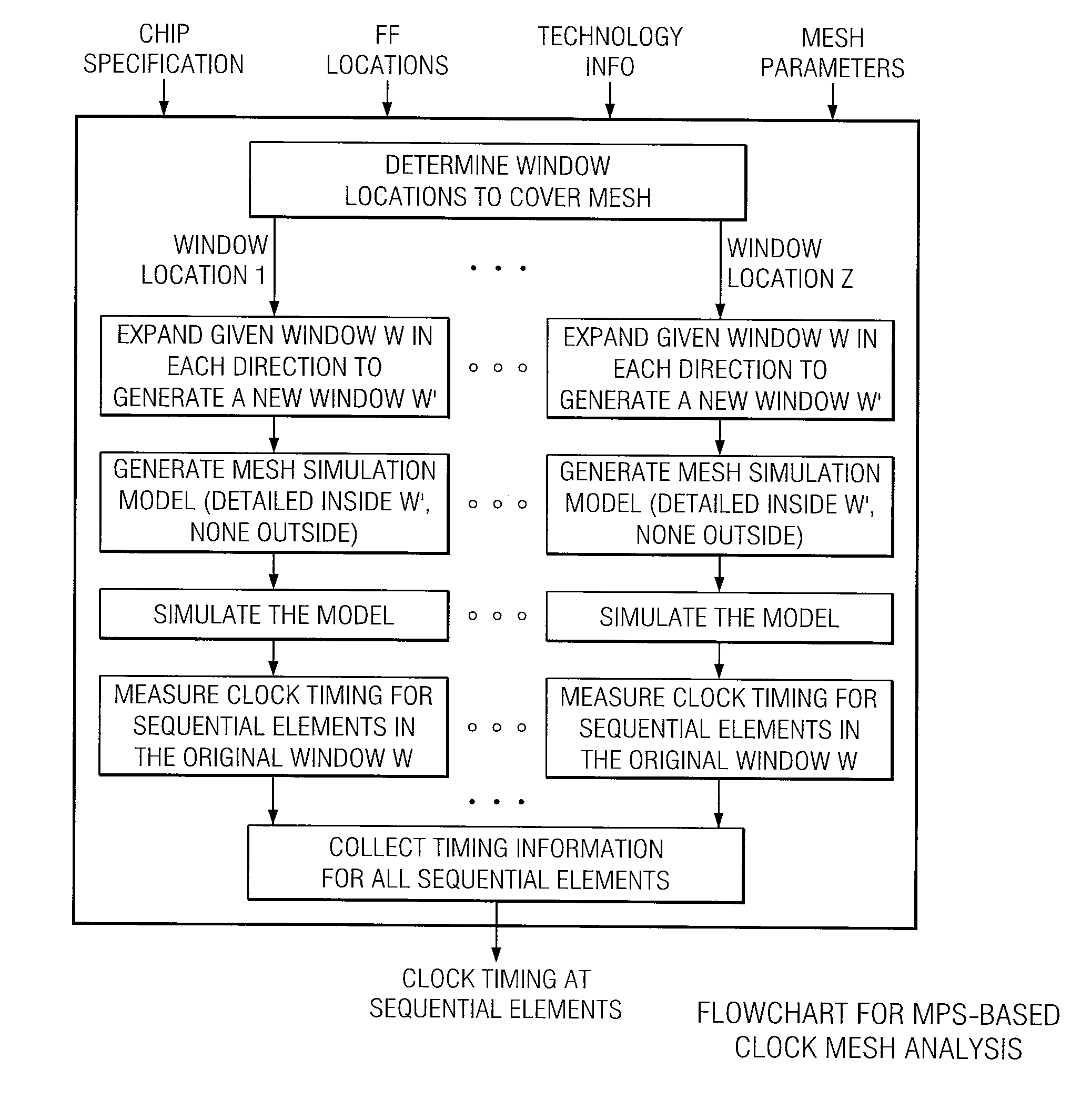
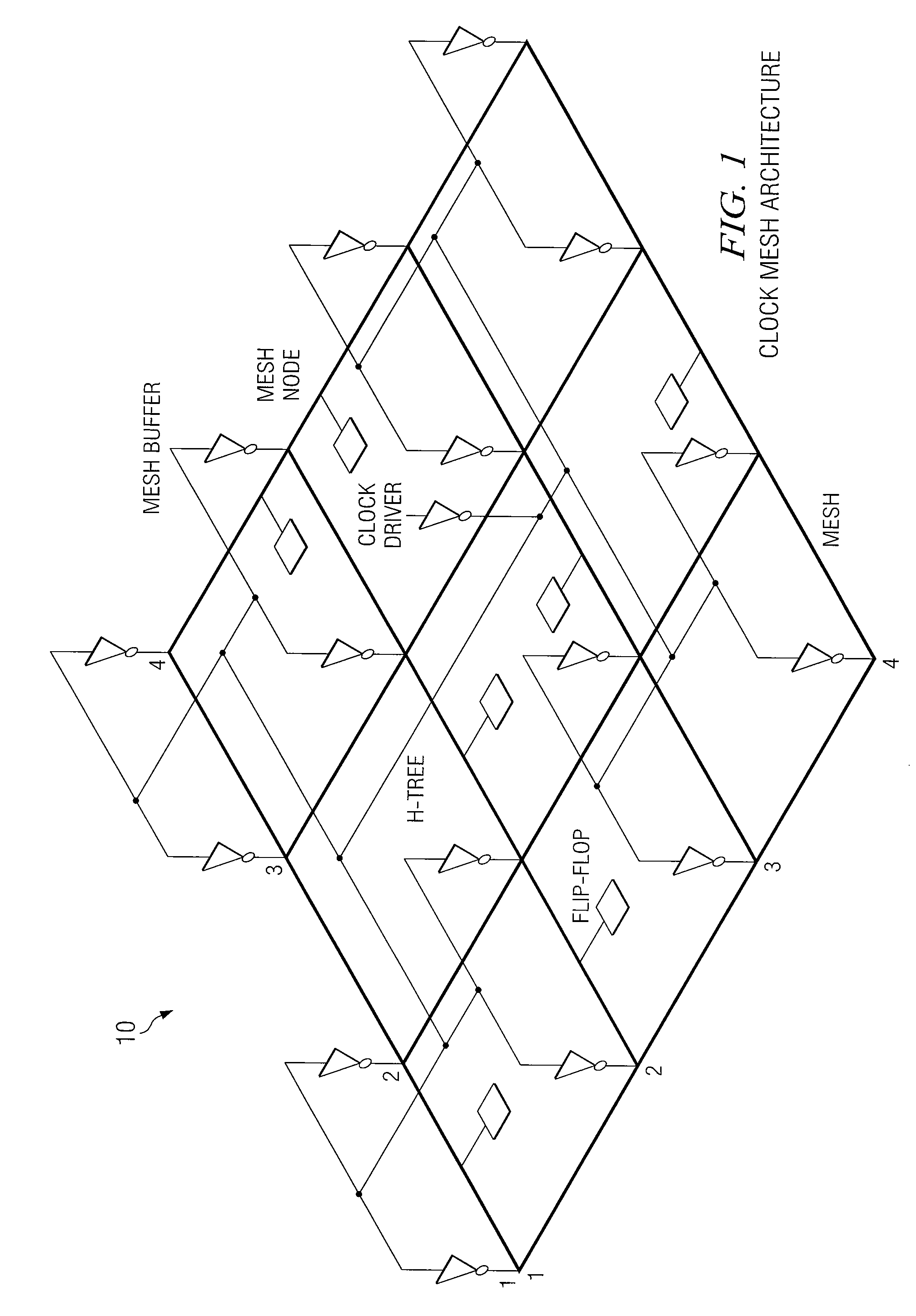
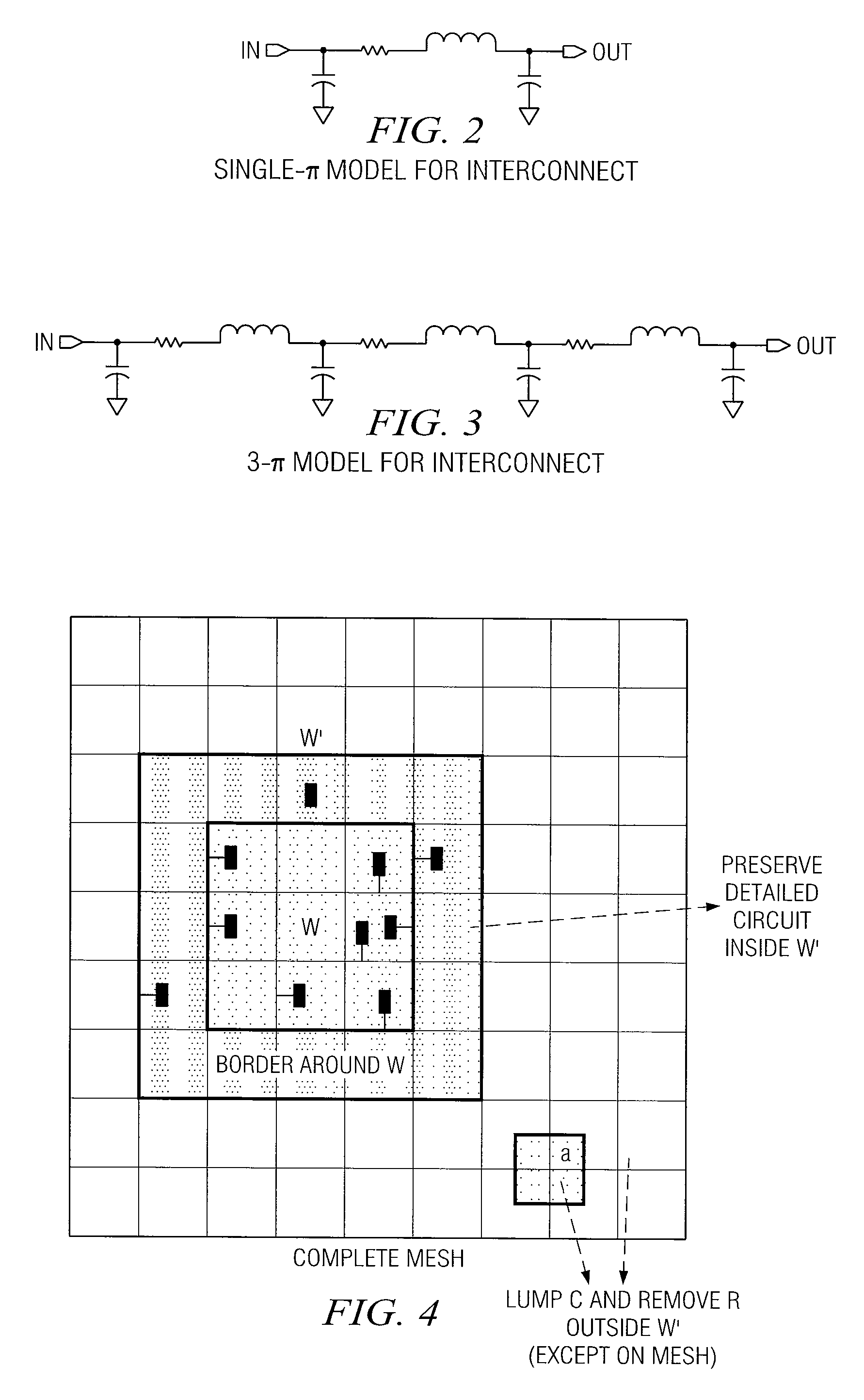
[0022]FIG. 1 is a simplified diagram of a typical or example mesh architecture system 10 used for distributing a clock signal from a phase lock loop (PLL) or root buffer to sequential elements such as flip-flops (FFs) and latches on the chip. It has three main components: 1) a (uniform) mesh, 2) a global buffered tree that drives the mesh, and 3) local interconnect, which connects the clock inputs of FFs directly to the nearest point on the mesh. The mesh is a uniform rectangular grid of wires spanning the entire chip area, driven by the mesh buffers and propagating the clock to the FFs. An m×n mesh or grid has m rows (horizontal wires) and n columns (vertical wires). The size of the mesh is m×n. For a given chip size, the greater the mesh size, the more fine-grain the mesh is. A mesh node (or grid node) is the point where each row is connected to each column. As shown in FIG. 1, the global (H−) tree delivers the clock signal to the mesh nodes via buffers called mesh buffers. We ass...


PUM


Abstract

A method is provided and includes accessing a description of a chip, which includes sequential elements and a clock mesh. Items used include: the description of the chip, the information for modeling the sequential elements and interconnections, and the set of parameters of the clock mesh. Additionally, the method includes determining a plurality of original window locations covering the clock mesh. Further, for each original window location, the method includes expanding the original window location in one or more directions to generate a larger window location; generating a mesh simulation model inside the larger window location; simulating the mesh simulation model; measuring clock timing for the sequential elements in the original window location based on the simulation of the mesh simulation model; and collecting timing information on all the sequential elements on the chip based on the measured clock timing for the sequential elements in the original window locations.

Description

RELATED APPLICATIONS[0001]This application claims the priority under 35 U.S.C. §119 of provisional application Ser. No. 60 / 804,041 filed Jun. 6, 2006.TECHNICAL FIELD OF THE INVENTION[0002]This invention relates in general to the field of clock meshes and, more particularly, to a system and a method for providing an improved sliding window scheme for clock mesh analysis.BACKGROUND OF THE INVENTION[0003]The proliferation of integrated circuits has placed increasing demands on the design of digital systems and microprocessors included in many devices, components, and architectures. The number of digital systems that include microprocessors continues to steadily increase and is driven by a wide array of products and systems. Added functionalities may be implemented in integrated circuits in order to execute additional tasks or to effectuate more sophisticated operations in their respective applications or environments.[0004]In the context of microprocessors, present generation embedded ...

Claims


Application Information

Patent Timeline
Patent Type & Authority Patents(United States)
IPC IPC(8): G06F17/50
CPCG06F1/10G06F17/5031G06F2217/62G06F30/3312G06F30/396
Inventor REDDY, SUBODH M.MURGAI, RAJEEV
Owner FUJITSU LTD
Why Eureka
Try Eureka