Electro-optical device with light shielding portion comprising laminated colored layers, electrical equipment having the same, portable telephone having the same

a technology of optical devices and light shielding portions, applied in the field of electromagnetic devices, can solve the problems of increased manufacturing steps, reduced signal delay, and formation of parasitic capacitance with other wirings

Inactive Publication Date: 2010-09-28
SEMICON ENERGY LAB CO LTD
View PDF70 Cites 24 Cited by
  • Summary
  • Abstract
  • Description
  • Claims
  • Application Information

AI Technical Summary

Problems solved by technology

In a conventional liquid crystal display device using a metallic film as a light shielding mask of a color filter, the problem in that a parasitic capacitance with other wirings is formed and delay in signals tends to occur.
Furthermore, in the case that an organic film containing a black pigment is used as a light shielding mask of a color filter, a problem in that the manufacturing steps increase occurs.

Method used


Image

  • Electro-optical device with light shielding portion comprising laminated colored layers, electrical equipment having the same, portable telephone having the same
  • Electro-optical device with light shielding portion comprising laminated colored layers, electrical equipment having the same, portable telephone having the same
  • Electro-optical device with light shielding portion comprising laminated colored layers, electrical equipment having the same, portable telephone having the same

Examples


embodiment 1

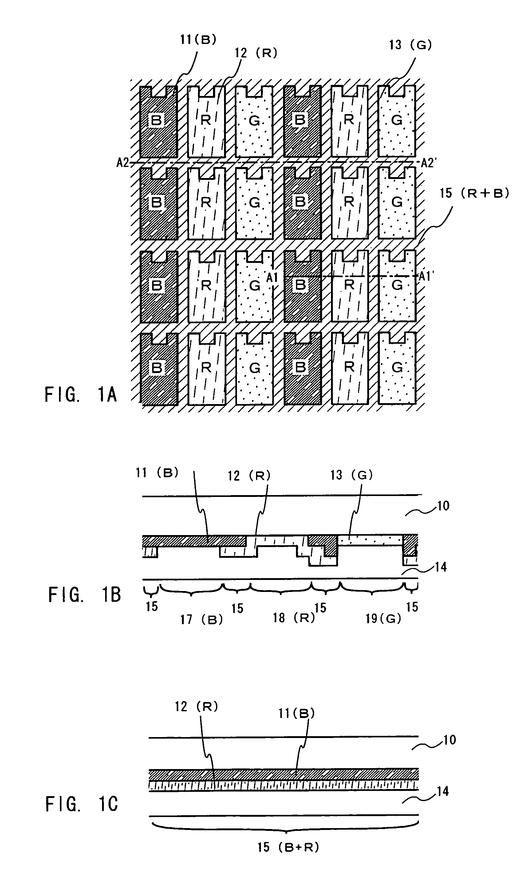
[0061]An embodiment of the present invention will be described hereinbelow with taking as an example a manufacturing of an opposing substrate which will be employed for an active matrix liquid crystal display device. FIG. 1 shows a schematic view of an opposing substrate with a colored layer formed according to this invention.

[0062]First, as an opposing substrate 10 having light transmission property, a glass substrate such as barium borosilicate glass or aluminum borosilicate, represented by such as Corning #7059 glass or #1737 glass is prepared. In addition to the above, a light transmission type substrate such as a quartz substrate and a plastic substrate may also be used.

[0063]Next, an organic photosensitive material (CRY-8000: color mosaic made by Fuji Film Olin Corp.) is applied on the opposing substrate 10, and by photolithography this organic photosensitive material is patterned in a grid-shape as shown in FIG. 1A to form a green colored layer (G) 13. Note that this region b...

embodiment 2

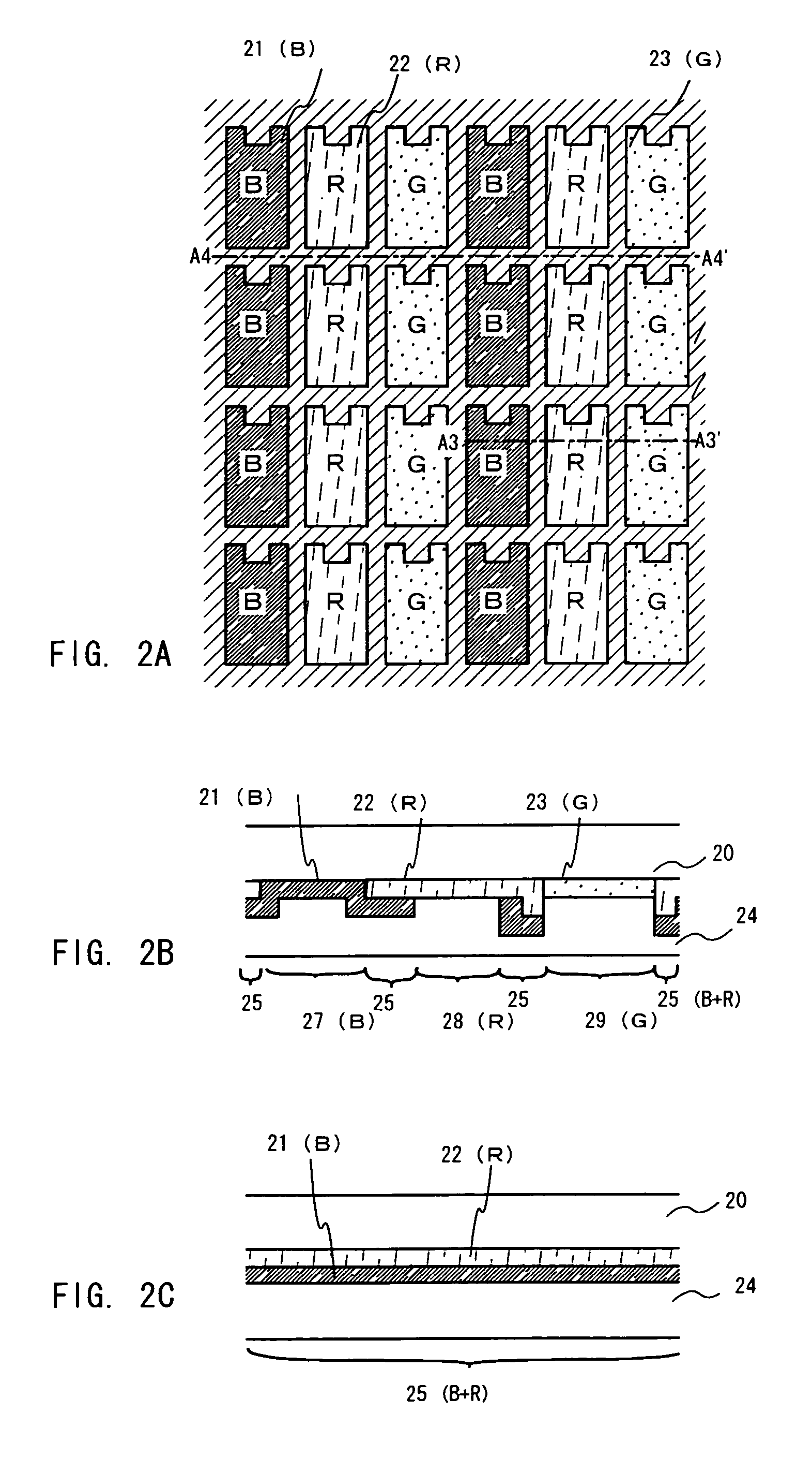
[0072]In Embodiment 1, an example where the green colored layer (G) 13, the blue colored layer (B) 11, the red colored layer (R) 12 are sequentially formed is shown, but an example where the colored layers are formed in a order different from that of Embodiment 1 is shown below.

[0073]FIG. 2A shows an example where first a colored layer (G) 23 is formed and then is laminated with a colored layer (R) 22 and a colored layer (B) 21. Note that, FIG. 2B corresponds to a cross sectional structural diagram cut along the chain line A3 to A3′ of FIG. 2A, and FIG. 2C corresponds to a cross sectional structural diagram cut along the chain line A4 to A4′ of FIG. 2A.

[0074]As an opposing substrate 20, the substrate adopted in Embodiment 1 is used.

[0075]First, an organic photosensitive material (CRY-8000: color mosaic made by Fuji Film Olin Corp.) is applied on the opposing substrate 20, and by photolithography this organic photosensitive material is patterned in a grid-shape as shown in FIG. 2A to...

embodiment 3

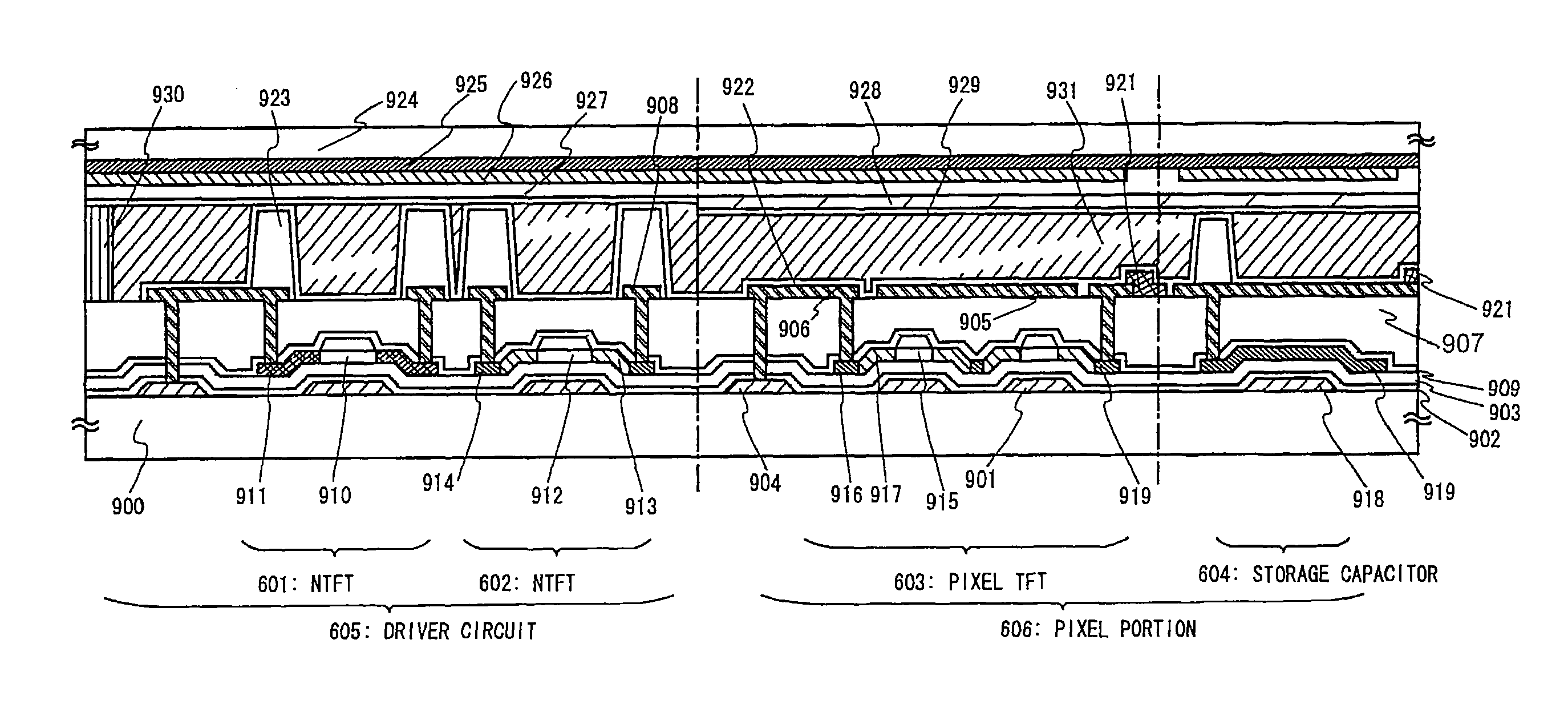
[0085]In this embodiment, a method of manufacturing an active matrix substrate is described with reference to FIGS. 5 to 11.

[0086]In this embodiment, a description will be made of a manufacturing method of an active matrix substrate (also referred to as device substrate) which is stuck with an opposing substrate obtained in Embodiment 1 or Embodiment 2. Here, a method of simultaneously forming, on the same substrate, a pixel portion and TFTs (n-channel TFT and p-channel TFT) of a driver circuit formed in the periphery of the pixel portion, is described in detail.

[0087]First, in this embodiment, a substrate 400 is used, which is made from glass, such as barium borosilicate glass or aluminum borosilicate glass, represented by such as Corning #7059 glass and #1737 glass. Note that, as the substrate 400, a quartz substrate may be used as the replace. A plastic substrate having heat resistance to a process temperature of this embodiment may also be used. There is no particular limitation...


PUM

PropertyMeasurementUnit
thicknessaaaaaaaaaa
transmittivityaaaaaaaaaa

Abstract

An object of the present invention is to provide a pixel structure capable of shielding light between a TFT and a pixel without using a light shielding mask (black matrix) in an electro-optical display device. The present invention has a feature in that, as one of means for shielding light, a lamination film consisting of two colored layers (a lamination layer of a red-colored layer and a blue-colored layer) is formed on an opposing substrate as a light shielding portion so as to overlap with a TFT formed on a device electrode.

Description

BACKGROUND OF THE INVENTION[0001]1. Field of the Invention[0002]The present invention relates to a semiconductor device having a circuit constructed of a thin film transistor (hereinafter referred to as TFT), and to a method of manufacturing the same. For example, the present invention relates to an electro-optical device, which is represented by a liquid crystal display device, and to electronic equipment loaded with the electro-optical device as a part.[0003]Note that, in this specification, the term semiconductor device indicates general devices that function by utilizing semiconductor characteristics, and that electro-optical devices, semiconductor circuits and electronic equipment are all included in the category of the semiconductor device.[0004]2. Description of the Related Art[0005]In recent years, a technique for constructing a thin film transistor (hereinafter referred to as TFT) using a semiconductor thin film (on the order of several to several hundreds nm in thickness) ...

Claims


Application Information

Patent Timeline
Patent Type & Authority Patents(United States)
IPC IPC(8): G02F1/1343G02F1/1335G02F1/136G02F1/1362H01L21/336H01L21/77H01L21/84H01L27/12H01L27/146H01L29/786
CPCG02F1/133512H01L27/1214H01L29/78633H01L27/14621H01L27/14623H01L29/66757H01L27/14609G02F1/133514G02F1/13454H01L27/1259H01L27/127
Inventor YAMAZAKI, SHUNPEIGOTO, YUUGOKATSURA, HIDEKI
Owner SEMICON ENERGY LAB CO LTD
Why Eureka
Try Eureka