Device and method for etching a substrate using an inductively coupled plasma

a technology of inductively coupled plasma and substrate, which is applied in the direction of plasma technique, electric discharge tube, decorative arts, etc., can solve the problems of unstable plasma injection, adversely affecting the etching results on the substrate wafer, and affecting the etching results, so as to improve the efficiency of reactive species and ions generation, the effect of improving the profile control during etching and plasma density

Inactive Publication Date: 2010-10-12
ROBERT BOSCH GMBH
View PDF32 Cites 25 Cited by
  • Summary
  • Abstract
  • Description
  • Claims
  • Application Information

AI Technical Summary

Benefits of technology

[0008]In contrast to the known methods, the device according to the present invention and the method implemented with it has the advantage that a variably adjustable, pulsed radio-frequency power is generated with it which can be injected into the inductively coupled plasma as a plasma power, it being possible for the pulsing of the plasma power to take place very rapidly, within microseconds for example, and simultaneously being combined with power changes of several thousand watts.
[0009]In addition, the implemented pulsing of the plasma power is associated with an essential improvement in the efficiency of the ICP source and opens up the possibility to reduce the mean plasma power without a reduction in the etching rate or to increase the etching rate with an unaltered mean plasma power. Moreover, pulsing of the plasma power makes it possible to effectively reduce electrical disturbance effects from the source area of the ICP source.

Problems solved by technology

However, these injectable plasma powers are subject to limits resulting firstly from the load carrying capacity of the electrical components and secondly from the nature of the process.
Consequently, high radio-frequency powers of the inductive plasma source, i.e., high plasma powers to be injected, intensify harmful electrical effects from the source area on the produced inductively coupled plasma which adversely affect the etching results on the substrate wafer.
In addition, in etching processes of the type described in German Patent 42 41 045 C2, with very high plasma powers, stability problems also occur in injecting the plasma during the switching phases between etching and passivation steps.
This stems from the fact that power reflection and overvoltage occurring with high powers in the kilowatt range to be injected during the switching phases have a destructive effect on the electrical circuit of the plasma source (coil, connected capacitors, generator output stages, etc.).
However, for this source type as well, the practicable power limit ranges from approximately 3 kilowatts to 5 kilowatts, above which the required radio-frequency components become extremely expensive or problems with regard to plasma stability become excessive.
Faster changes in power are not possible with this approach.

Method used


Image

  • Device and method for etching a substrate using an inductively coupled plasma
  • Device and method for etching a substrate using an inductively coupled plasma
  • Device and method for etching a substrate using an inductively coupled plasma

Examples


Embodiment Construction

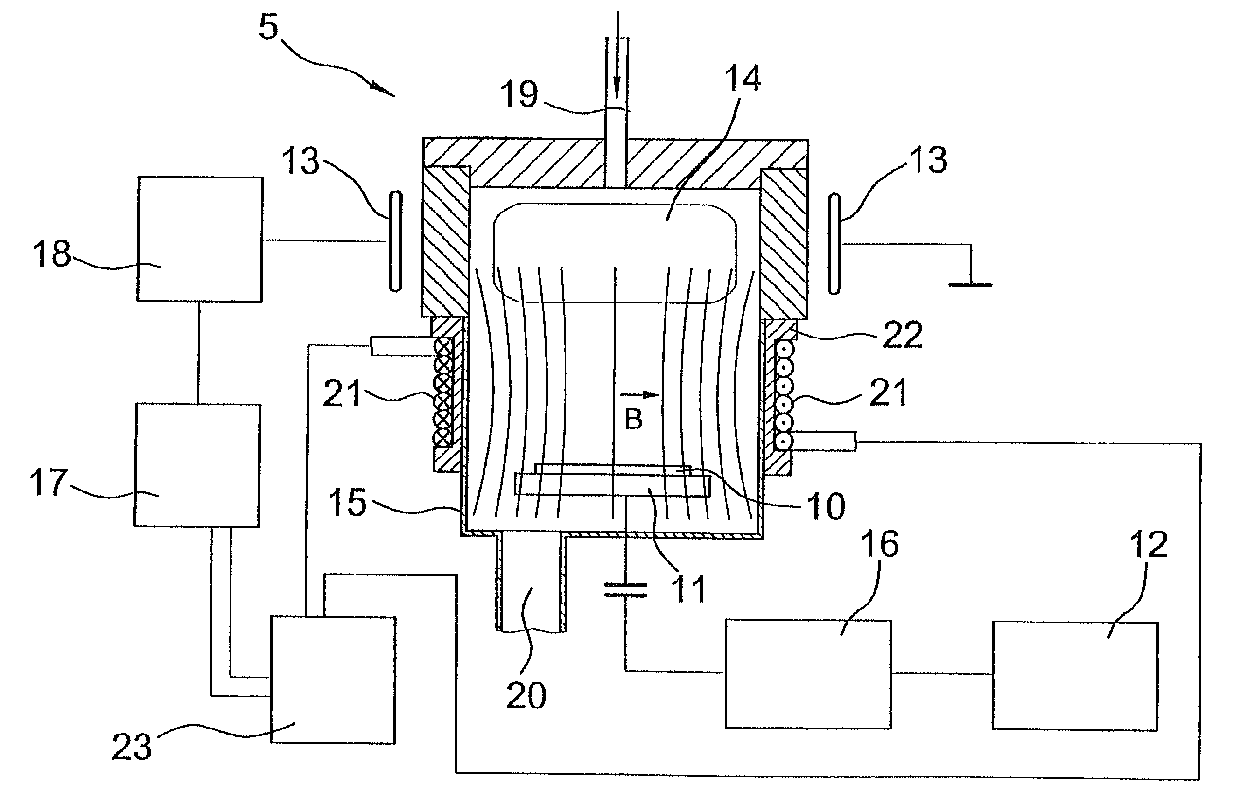
[0031]A first exemplary embodiment of the present invention is explained in greater detail with reference to FIG. 1. For this purpose, a plasma etching system 5 first has a reactor 15, in whose upper area an inductively coupled plasma 14 is generated in a manner known per se via an ICP source 13 (inductively coupled plasma). Additionally provided are a gas supply 14 for the supply of a reactive gas such as SF6, ClF3, O2, C4F8, C3F6, SiF4 or NF3, a gas discharge 20 for the discharge of reaction products, a substrate 10, for example, a silicon body or silicon wafer to be structured using the etching method of the present invention, a substrate electrode 11 being in contact with substrate 10, a substrate voltage generator 12, and a first impedance transformer 16. Substrate voltage generator 12 injects a high-frequency AC voltage into substrate electrode 11 and through it into substrate 10, the high-frequency AC voltage bringing about an acceleration of ions produced in inductively coup...


PUM

PropertyMeasurementUnit
frequencyaaaaaaaaaa
poweraaaaaaaaaa
radio-frequency poweraaaaaaaaaa

Abstract

A method and a device suitable for implementing this method for etching a substrate (10), a silicon body in particular, using an inductively coupled plasma (14) are proposed. For this purpose, a radio-frequency electromagnetic alternating field is generated with an ICP source (13), the alternating field generating an inductively coupled plasma (14) of reactive particles in a reactor (15). The inductively coupled plasma (14) arises by the action of the radio-frequency electromagnetic alternating field on a reactive gas. Furthermore, a device is provided with which a plasma power injected into the inductively coupled plasma (14) via the radio-frequency electromagnetic alternating field with the ICP source (13) is capable of being pulsed so that at least from time to time a pulsed radio-frequency power can be injected into the inductively coupled plasma (14) as a pulsed radio-frequency power. In addition, the pulsed plasma power can be combined or correlated with a pulsed magnetic field and / or a pulsed substrate electrode power.

Description

FIELD OF THE INVENTION[0001]The invention relates to a device and a method which can be implemented with it for etching a substrate, a silicon body in particular, using an inductively coupled plasma according to the species of the independent claims.DESCRIPTION OF RELATED ART[0002]In order to implement an anisotropic high-rate etching method, for silicon for example, using an inductive plasma source, in methods such as those known from German Patent 42 41 045 C2, for example, it is necessary to bring about an efficient sidewall passivation in the shortest possible time during passivation steps and moreover to achieve as high a concentration as possible of silicon-etching fluorine radicals during etching steps. In order to increase the etching rate, an obvious step is to work with maximally high radio-frequency powers at the inductive plasma source and as a result, to inject maximally high plasma powers into the produced inductively coupled plasma.[0003]However, these injectable plas...

Claims


Application Information

Patent Timeline
Patent Type & Authority Patents(United States)
IPC IPC(8): H01L21/311C03C15/00H05H1/46H01J37/32H01L21/302H01L21/3065
CPCH01J37/321H01J37/3266H01L21/3065
Inventor BECKER, VOLKERLAERMER, FRANZSCHILP, ANDREA
Owner ROBERT BOSCH GMBH
Why Eureka
Try Eureka