Optical ultrasound device

a technology of optical ultrasound and ultrasound, applied in measurement devices, phase-affecting properties, instruments, etc., can solve the problems of limiting the applicability of the device, no single design that can incorporate multiple advantages, and affecting the signal to noise, so as to reduce electronic interference, improve signal to noise, and design compact

Inactive Publication Date: 2010-10-12
GARDNER JUDD
View PDF10 Cites 2 Cited by
  • Summary
  • Abstract
  • Description
  • Claims
  • Application Information

AI Technical Summary

Benefits of technology

[0008]An ultrasound detector based upon optical interferometry is described. The detector provides advantages of sensitivity, noise immunity and compact design. The device may be designed as an optically isolated sensor with all electronics located remotely from the point of measurement. In another embodiment the device is designed with all electronics incorporated on the same substrate as the sensor. The device may be used in a variety of modes. In one embodiment the device is a single element sensor composed of a piezoelectric transmit and receive element located on a single substrate. The same piezoelectric element is used as the acoustical signal receiver for the reflected pulse. Timing of the excitation and detection circuits is used to detect single pulse excitation. The fact that the device uses optical detection of the reflected pulse minimizes electronic interference from the excitation pulse and any other potential electromagnetic interference. In another configuration, a piezoelectric excitation element and a separate acoustical signal-receiving element are located on the same substrate. The device so configured may be operated in a continuous excitation and receiving mode. Acoustical sensors are often operated in an array to improve signal to noise and provide higher spatial resolution images. With multiple excitation sources and a structured excitation beam, acoustical sensors may provide three-dimensional imaging. The compact design of the invented sensors helps to facilitate multiple sensor imaging applications. The optical sensing avoids electrical cross talk amongst the multiple sensors when so used as well as electrical interference from any other electronic devices operating in the neighborhood of the testing. In another embodiment, multiple piezoelectric elements are located on the same substrate. Multiple piezoelectric elements may act both for excitation and for receiving the reflected acoustic signals. In one embodiment, multiple elements share the same optical interferometer detection device. The signal from individual sensor elements is sorted by timing sequences. In another embodiment, multiple individual optical sensors may be located on the same substrate. Dynamic steering of the excitation beam and dynamic focusing is enabled in this configuration.

Problems solved by technology

One disadvantage of such designs is that the electrical signal required for excitation of the piezoelectric device is generally several orders of magnitude larger than the electrically measured reflected signal using a piezoelectric detector.
Additionally, signal to noise often limits the applicability of the device.
The sensor may therefore be used in corrosive or otherwise dangerous environments.
There is, however, no single design that can incorporate the multiple advantages.

Method used


Image

  • Optical ultrasound device
  • Optical ultrasound device
  • Optical ultrasound device

Examples


Embodiment Construction

Description of the Devices

[0025]Detailed embodiments are described referring to the attached figures. The exemplary descriptions demonstrate the flexibility of the invented design. All possible combinations of the features described are not necessarily included but will be apparent to those skilled in the art. For example, separation of the excitation and detection components is possible with all of the devices, not just those where the feature is explicitly described. Other features likewise may be shared amongst the various designs. The detailed descriptions of the selected examples are in no way intended to limit the other possible combinations of features.

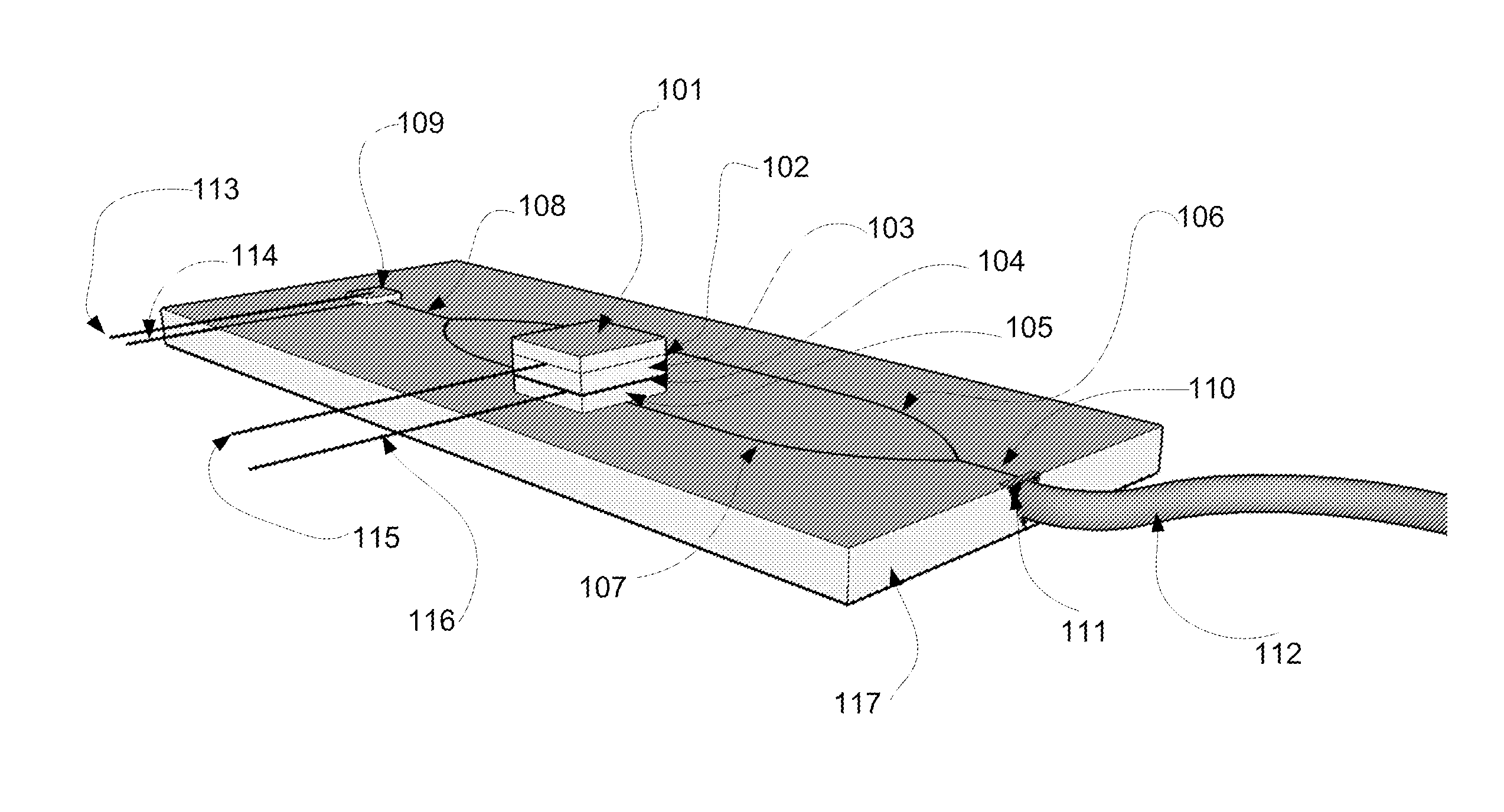
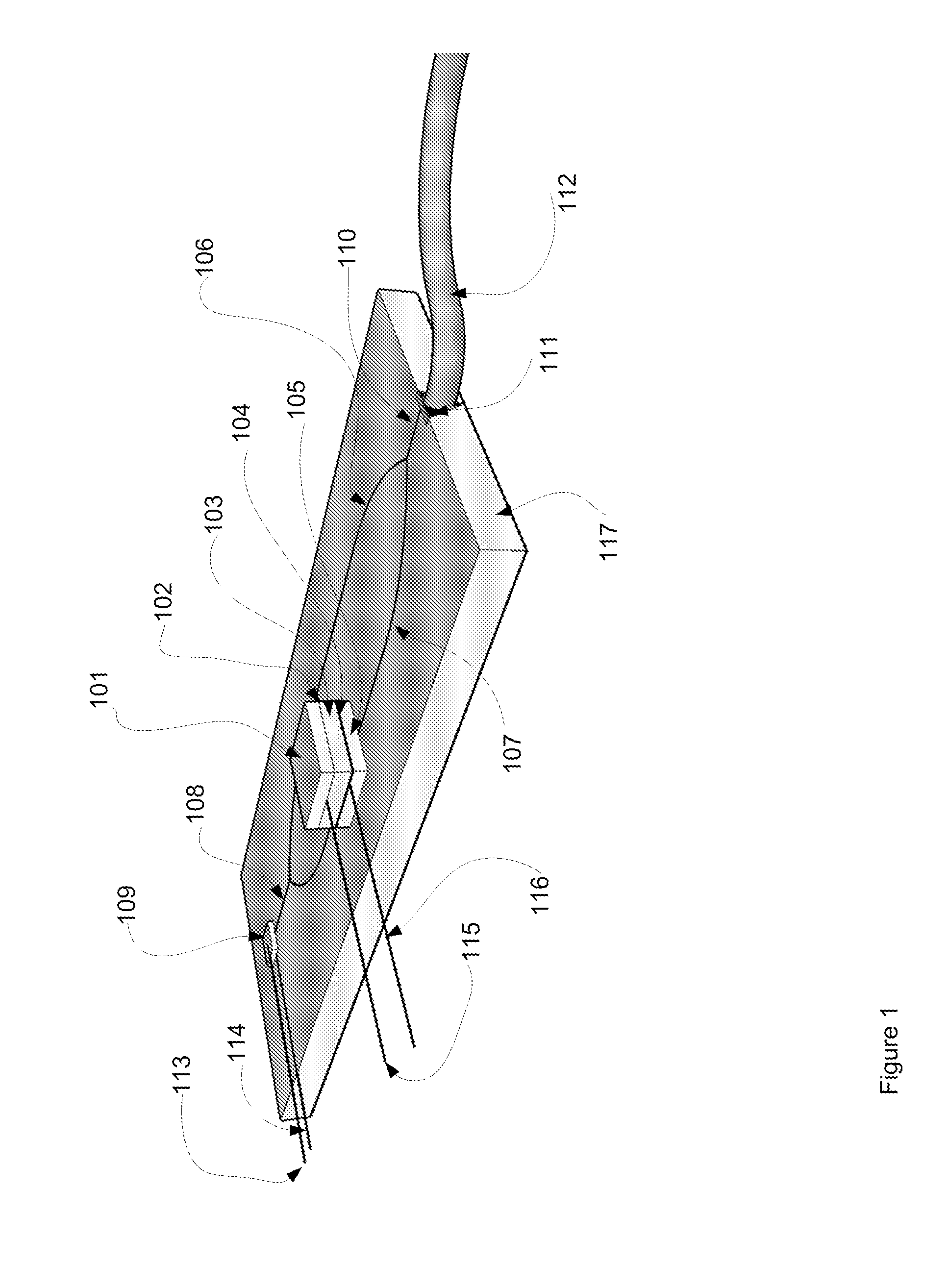
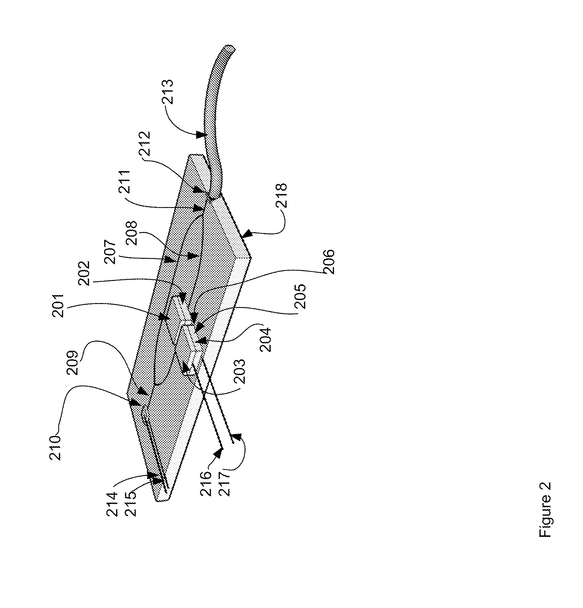
[0026]A single element transducer shown in FIG. 1 exhibits a stack composed of a matching layer 101, a top electrode 102, a piezoelectric element 103, a bottom electrode 104, and a backing layer 105. The stack is mounted on the top surface of the substrate 117 symmetrically over the modulated arm of a Mach-Zehnder interferomete...


PUM


Abstract

A new optical ultrasonic analysis transducer is described. The device includes a new detection means for the reflected ultrasound signal. The detector may be incorporated into a microchip design. The detector is compatible with a variety of material and design geometries that may be optimized for the particular application. Versions of the device may optionally include both excitation and receiving elements on the same device or these elements may be separate. Example designs are shown with applications to continuous wave ultrasound analysis useful for example in Doppler fluid flow measurements. Other designs are shown with multiple arrays and multiple excitation transducers to allow flexible three-dimensional imaging apparatus to be built. An equivalent circuit analysis of the frequency response and signal sensitivity provides means to customize material selection and other design parameters for particular applications.

Description

TECHNICAL FIELD[0001]Embodiments of the invention relate to an ultrasound device whose design may be modified so that it may be used in wide variety of ultrasonic imaging applications such as medical imaging and material testing purposes.BACKGROUND OF THE INVENTION[0002]Ultrasound imaging has been in wide use in a variety of industries. In the typical application, a piezoelectric element is used for both excitation and detection of the ultrasound signal. In a noninvasive use, such as the medical application of prenatal imaging, a piezoelectric element is placed in intimate contact with the pregnant woman's body to be tested and the element is excited with an electrical pulse with a center frequency selected for optimum penetration to the area of interest. The images allow assessment of the condition of the developing fetus. Arrays of sensors are often used to simplify data acquisition, improve spatial resolution, and improve signal to noise. Such arrays may also allow creation of a ...

Claims


Application Information

Patent Timeline
Patent Type & Authority Patents(United States)
IPC IPC(8): G01B9/02
CPCG01N21/1702G01N21/45G01N29/2437
Inventor GARDNER, JUDD
Owner GARDNER JUDD
Why Eureka
Try Eureka