Supercharge Your Innovation With Domain-Expert AI Agents!

Luminance improved organic electroluminescent device

a technology of organic electroluminescent devices and luminance, which is applied in the direction of luminescnet screens, discharge tubes, identification means, etc., can solve the problems of reducing affecting the overall luminance of the oled, and affecting the use of the current oled. achieve the effect of improving the luminance per pixel uni

Inactive Publication Date: 2010-10-19
SAMSUNG DISPLAY CO LTD
View PDF13 Cites 5 Cited by
  • Summary
  • Abstract
  • Description
  • Claims
  • Application Information

AI Technical Summary

Benefits of technology

The solution enhances luminance and extends the life cycle of OLEDs by increasing light coupling efficiency and reducing the need for additional driving voltage, while simplifying the fabrication process by eliminating the requirement for an additional mask process.

Problems solved by technology

Certain problems exist in the currently used OLED.
Most importantly, light emission is not satisfactory due to the escape of reflected light from the structure of the OLED.
As a result, the overall luminance of the OLED is reduced, and this provides a less efficient device.
Another problem with current OLED device is that its life is shortened due to the necessity to increase the driving voltage applied to it in order to compensate for the aforementioned reduced luminance.

Method used


Image

  • Luminance improved organic electroluminescent device
  • Luminance improved organic electroluminescent device
  • Luminance improved organic electroluminescent device

Examples


Embodiment Construction

[0022]The present invention will now be described in detail in connection with preferred embodiments with reference to the accompanying drawings. For reference, like reference characters will be used to designate corresponding parts throughout the several views.

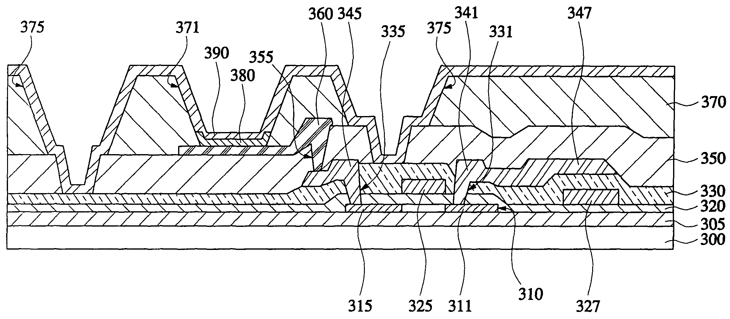
[0023]FIG. 1 is a cross sectional view of an active matrix organic light emitting diode (OLED).

[0024]Referring to FIG. 1, a buffer layer 105 is formed on an insulating substrate 100, and a thin film transistor and a capacitor are formed on the buffer layer 105. The thin film transistor comprises a semiconductor layer 110 which includes source / drain regions 111 and 115, a gate electrode 125 formed on a gate insulating film 120, and source / drain electrodes 141 and 145 formed on an interlayer insulating film 130 and connected to the source / drain regions 111 and 115 through contact holes 131 and 135. The capacitor comprises first electrode 127 formed of the same material as the gate electrode 125 and formed on the gate insulating...


PUM


Abstract

An organic light emitting diode (OLED) is capable of improving light efficiency per pixel unit by forming a cathode electrode to cover an anode electrode, thereby focusing light emitted from a luminescent layer per pixel unit. The OLED comprises: a second insulating film formed on a substrate including a TFT with source / drain electrodes formed on a first insulating film; a lower electrode formed on the second insulating film and connected to one of the source / drain electrodes; a third insulating film having an opening for exposing a portion of the lower electrode; a luminescent layer formed on the lower electrode inside the opening; a groove formed to surround the luminescent layer; and an upper electrode formed on the substrate including the groove so that the upper electrode surrounds the luminescent layer. The upper electrode functions as a reflection layer for reflecting total light while light emitted from the luminescent layer is being pulled out through the substrate.

Description

CLAIM OF PRIORITY AND CROSS-REFERENCE TO RELATED APPLICATION[0001]This application makes reference to, incorporates the same herein, and claims all benefits accruing under 35 U.S.C. §119 from an application for OELD WITH IMPROVED BRIGHTNESS earlier filed in the Korean Intellectual Property Office on 20 Dec. 2002 and there duly assigned Serial No. 2002-81856. Furthermore, this application is a divisional of Applicants' Ser. No. 10 / 683,353 filed in the U.S. Patent & Trademark Office on 14 Oct. 2003 now U.S. Pat. No. 7,391,151 and assigned to the assignee of the present invention.BACKGROUND OF THE INVENTION[0002]1. Technical Field[0003]The present invention relates to an active matrix flat panel display and, more particularly, to an organic light emitting diode capable of improving luminance per pixel unit by forming a cathode electrode which surrounds an organic luminescent layer, thereby focusing light per pixel unit.[0004]2. Related Art[0005]Generally, light efficiency of an organic...

Claims


Application Information

Patent Timeline
Patent Type & Authority Patents(United States)
IPC IPC(8): H05B33/26G09F9/30H01L27/32H01L51/50H01L51/52H05B33/00H05B33/02H05B33/10H05B33/12H05B33/14H05B33/22
CPCH01L51/5271H01L27/3244H01L51/5221H10K59/12H10K59/8052H10K59/878H05B33/26H10K50/856H10K50/82
Inventor KOO, JAE-BONPARK, JIN-WOO
Owner SAMSUNG DISPLAY CO LTD
Features
  • R&D
  • Intellectual Property
  • Life Sciences
  • Materials
  • Tech Scout
  • Unparalleled Data Quality
  • Higher Quality Content
  • 60% Fewer Hallucinations
Learn More