Photocathode comprising a plurality of openings on an electron emission layer

a photocathode and electron emission layer technology, applied in the field of photocathodes, can solve the problems of not having sensitivity to visible laser light wavelengths as well as wavelengths of ultraviolet band

Inactive Publication Date: 2010-10-19
HAMAMATSU PHOTONICS KK
View PDF20 Cites 47 Cited by
  • Summary
  • Abstract
  • Description
  • Claims
  • Application Information

AI Technical Summary

Benefits of technology

[0017]The above-described semiconductor photocathode may furthermore include: a contact layer, interposed between the electron emission layer and the second electrode and formed of a semiconductor material that is lattice matched to the electron emission layer. Because by providing a contact layer, a contact resistance between the electron emission layer and the second electrode can be lowered, the bias voltage can be applied effectively.
[0018]The above-described semiconductor photocathode may furthermore include: an insulating film, interposed between the transparent substrate and the first electrode. By providing such an insulating film, an effect of improving the adherence of the transparent substrate and semiconductor materials is provided.
[0019]The above-described semiconductor photocathode may furthermore include: an antireflection film, interposed between the transparent substrate and the first electrode. By providing the antireflection film, reflectance at desired wavelengths can be reduced in regard to light that is made incident on the light absorbing layer and the photoelectron emission efficiency can be improved.

Problems solved by technology

However, because the photocathode described in Patent Document 1 is narrow in the wavelength band of incident light that can excite photoelectrons, though the photocathode has adequate sensitivity to wavelengths of infrared fluorescence, it does not have sensitivity to wavelengths of visible laser light as well as wavelengths of an ultraviolet band.

Method used


Image

  • Photocathode comprising a plurality of openings on an electron emission layer
  • Photocathode comprising a plurality of openings on an electron emission layer
  • Photocathode comprising a plurality of openings on an electron emission layer

Examples


first embodiment

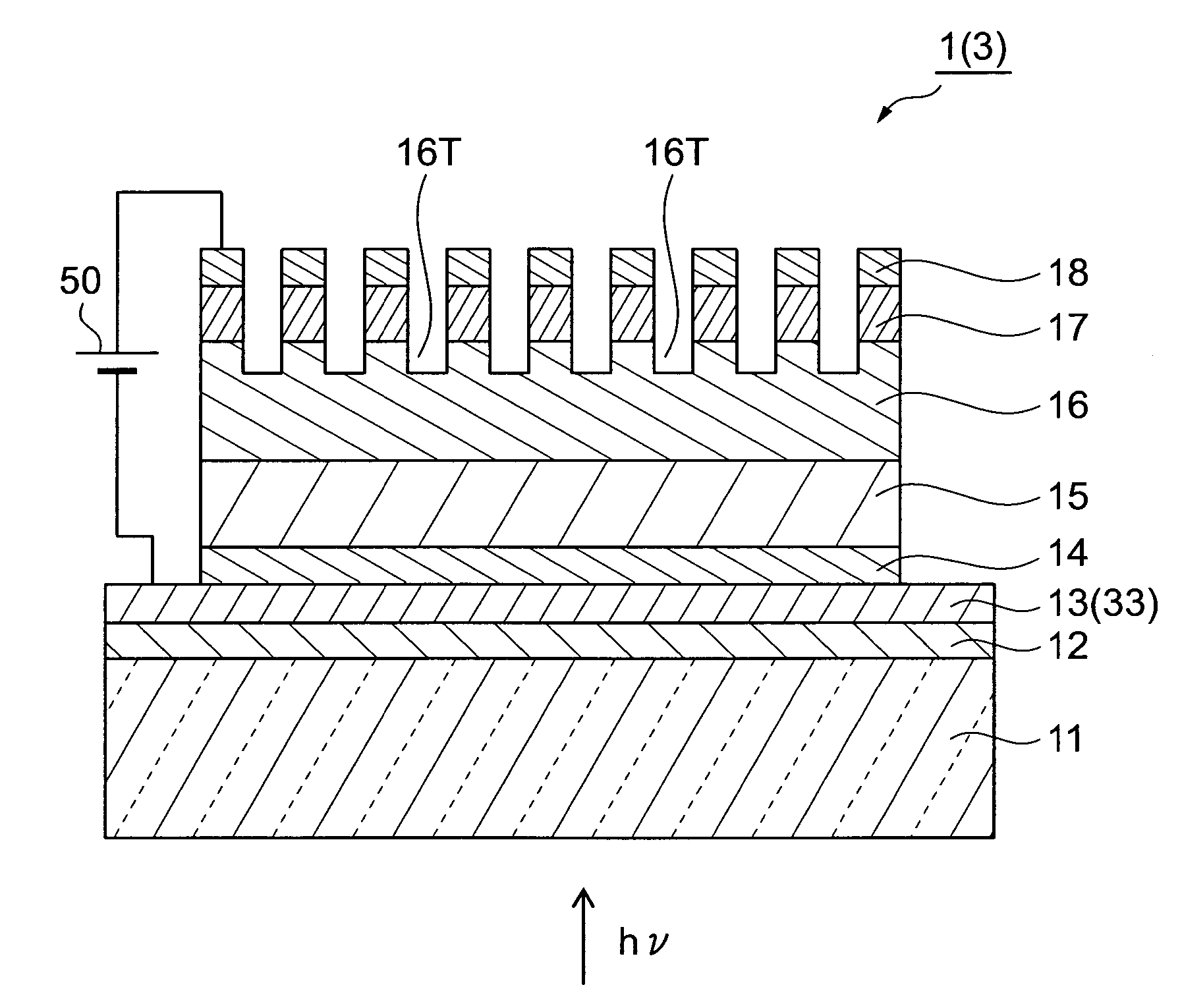
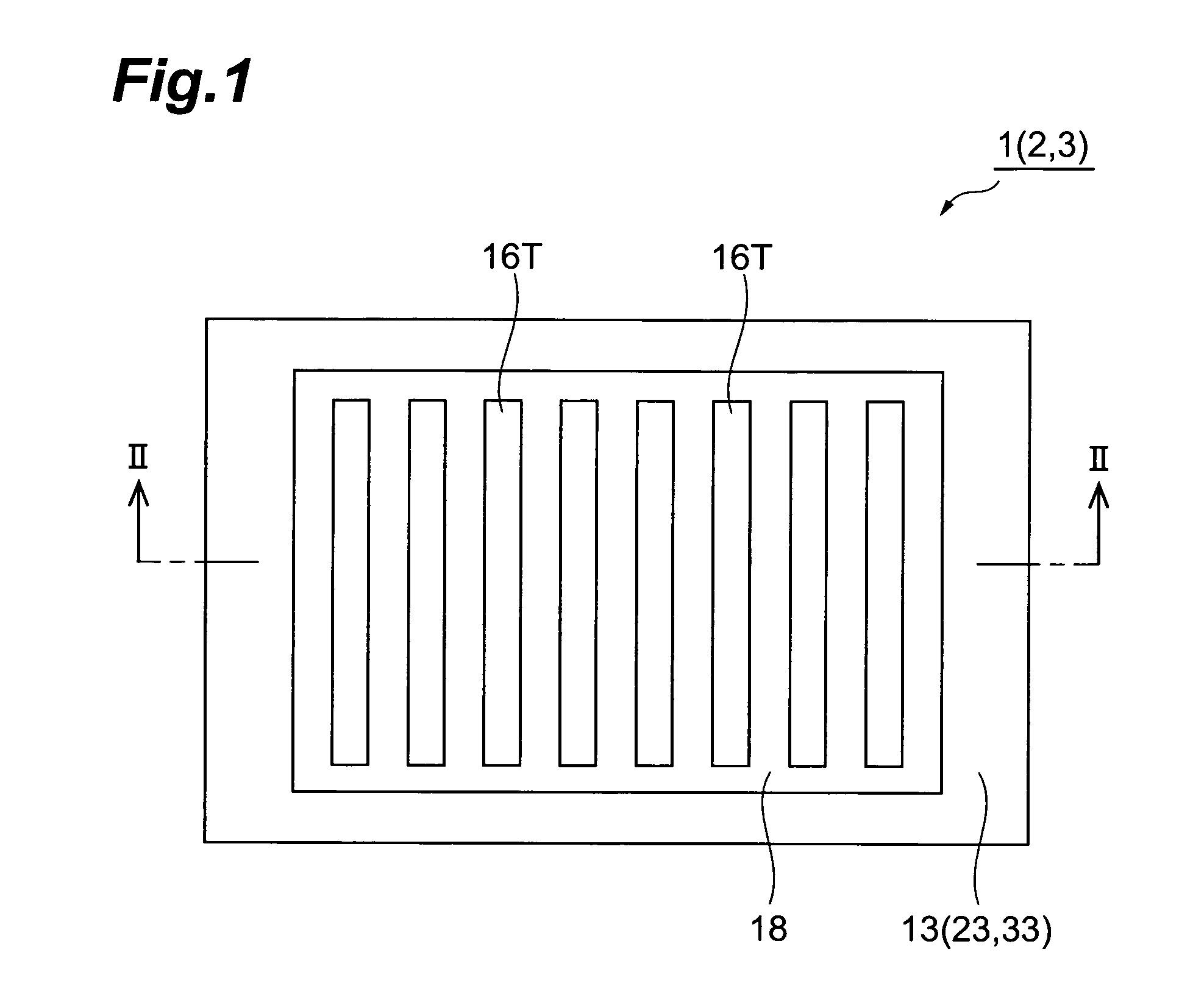
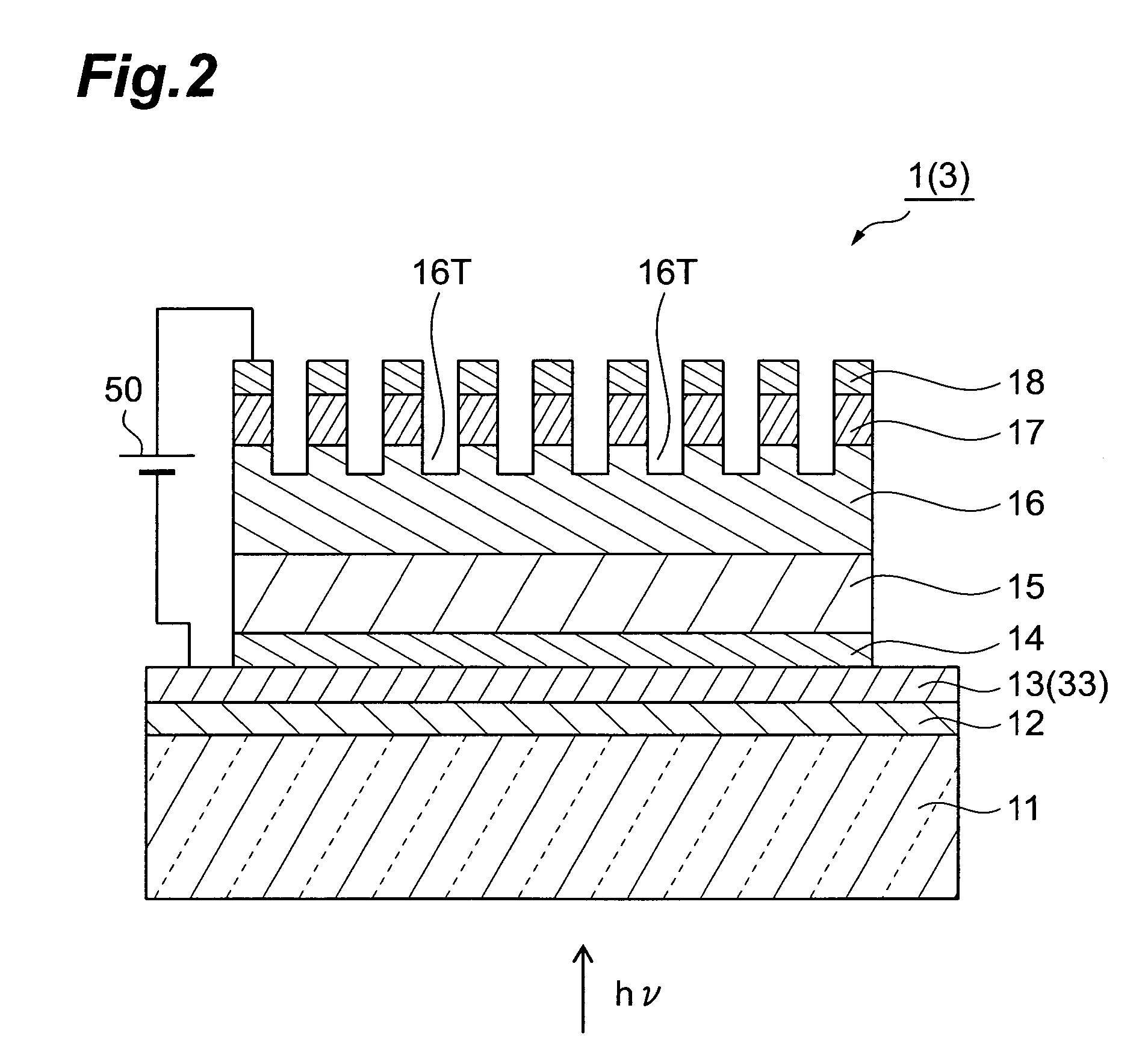
[0029]FIG. 1 is a plan view of a transmission-type semiconductor photocathode 1 according to a first embodiment, and FIG. 2 is a sectional view taken on line II-II of FIG. 1.

[0030]The semiconductor photocathode 1 includes a transparent substrate 11, an intermediate film (insulating film or antireflection film) 12, a first electrode 13, a window layer 14, a light absorbing layer 15, an electron emission layer 16, a contact layer 17, and a second electrode 18. The window layer 14, the light absorbing layer 15, the electron emission layer 16, and the contact layer 17 are arranged as a semiconductor multilayer film that serves the role of photoelectric conversion.

[0031]The transparent substrate 11 is formed of a material that is not restricted in the short wavelength sensitivity end and transmits an incident light hv of a wide wavelength band spanning from an ultraviolet band to a near infrared band. As the material of the transparent substrate 11, for example, glass or quartz is used. ...

second embodiment

[0059]A transmission-type semiconductor photocathode according to a second embodiment of the present invention shall now be described.

[0060]FIG. 6 is a sectional view of the transmission-type semiconductor photocathode 2 according to the second embodiment. Because the plan view of the semiconductor photocathode 2 is the same as FIG. 1, description shall be omitted by providing elements corresponding to those of FIG. 1 with the same symbols.

[0061]A difference of the present embodiment with respect to the first embodiment is a first electrode 23 that is disposed at the light incidence side, and other elements are the same as those of the first embodiment. With the present embodiment, the first electrode 23 differs from that of the first embodiment in being arranged as a metal material layer having openings 23B. Specifically, as shown in the plan view of FIG. 7, by providing the plurality of openings 23B in the first electrode 23, the first electrode 23 is patterned in the form of stri...

third embodiment

[0068]A transmission-type semiconductor photocathode according to a third embodiment shall now be described. Because the semiconductor photocathode according to the present embodiment is the same as the first embodiment in plan view and sectional view, corresponding elements shall be provided with the corresponding symbols and description thereof shall be omitted.

[0069]A difference between the present embodiment and the first embodiment is a first electrode 33 that is disposed at the light incidence side of the semiconductor photocathode 3 (see FIG. 2), and other elements are the same as those of the first embodiment. Specifically, the present embodiment differs from the first embodiment in that the first electrode 33 is formed of a transparent conductive material. The transparent conductive material making up the first electrode 33 may be at least one type of material selected from the group consisting of ITO, ZnO, In2O3, and SnO2. ITO, ZnO, In2O3, and SnO2 are all transparent oxid...


PUM


Abstract

A semiconductor photocathode 1 includes: a transparent substrate 11; a first electrode 13, formed on the transparent substrate 11 and enabling passage of light that has been transmitted through the transparent substrate 11; a window layer 14, formed on the first electrode 13 and formed of a semiconductor material with a thickness of no less than 10 nm and no more than 200 nm; a light absorbing layer 15, formed on the window layer 14, formed of a semiconductor material that is lattice matched to the window layer 14, is narrower in energy band gap than the window layer 14, and in which photoelectrons are excited in response to the incidence of light; an electron emission layer 16, formed on the light absorbing layer 15, formed of a semiconductor material that is lattice matched to the light absorbing layer 15, and emitting the photoelectrons excited in the light absorbing layer 15 to the exterior from a surface; and a second electrode 18, formed on the electron emission layer.

Description

BACKGROUND OF THE INVENTION[0001]1. Field of the Invention[0002]The present invention relates to a photocathode.[0003]2. Related Background Art[0004]Photocathodes are used in photodetectors and other measuring devices, and for example, a transmission type photocathode, described in (Patent Document 1: Japanese Published Unexamined Patent Application No. H9-199075) is used. This transmission type photocathode is sensitive to near infrared light and has a window layer, formed of InAlGaAs on a light incidence side of a light absorbing layer, formed of an InGaAs-based material.[0005]With photocathodes, forming of a transparent conductive film on a light incidence side of a light absorbing layer to lower a surface resistance that obstructs analysis of high-speed phenomena, etc., using a photodetector is known (see Patent Document 2: Japanese Published Examined Patent Application No. H4-30706). The provision of a mesh electrode or an island electrode at a light incidence side to apply a b...

Claims


Application Information

Patent Timeline
Patent Type & Authority Patents(United States)
IPC IPC(8): H01J40/06G21K5/10H01L29/12H01J37/08
CPCH01J1/34H01J2201/3423
Inventor NAKAJIMA, KAZUTOSHINIIGAKI, MINORUMOCHIZUKI, TOMOKOHIROHATA, TORU
Owner HAMAMATSU PHOTONICS KK
Why Eureka
Try Eureka