Programmable resistance memory element and method for making same

a memory element and resistance technology, applied in the field of memory elements, can solve the problems of limited direct and universal replacement use of memory elements, high energy requirements needed to program the resistance of memory elements, and inconsequential power saving, and achieve the effect of reducing the energy requirements for the programming of elements

Inactive Publication Date: 2010-11-16
OVONYX MEMORY TECH LLC
View PDF6 Cites 76 Cited by
  • Summary
  • Abstract
  • Description
  • Claims
  • Application Information

AI Technical Summary

Benefits of technology

[0009]An aspect of the present invention is an improved programmable resistance memory element in which the energy requirements for the programming of the element may be reduced. This may be accomplished by a programmable memory element comprising a region of conductive material embedded in a first region of dielectric material deposited upon a substrate. The conductive material is adapted to receive an electrical input signal from a signal source. The element also includes a sidewall layer of memory material embedded in a second dielectric region deposited upon the first region, a bottom surface of the sidewall layer of memory material is in electrical communication with a top surface of the region of conductive material. The memory material is preferably formed as a sidewall spacer of memory material. The top surface of the conductive material and the bottom surface of the memory material preferably form only one area of contact. The area of contact preferably has dimensions corresponding to a width of the top surface of the conductive material and a width of the bottom surface of the memory material. The width of the top surface of the conductive material and the width of the bottom surface of the memory material may each be non-lithographically defined.
[0011]Another aspect of the present invention is a method of forming a programmable resistance memory element in such a way that the programming energy requirement for the element may be reduced. The method of forming the programmable memory element comprises the step of embedding a region of conductive material in a first region of dielectric material deposited upon a substrate, the conductive material adapted to receive an electrical input signal from a signal source. The method further includes the step of embedding a sidewall layer of memory material in a second dielectric region deposited upon the first region, a bottom surface of the sidewall layer of memory material in electrical communication with a top surface of the region of conductive material. The memory material is preferably in the form of a sidewall spacer of memory material. The top surface and the bottom surface preferably form only one area of contact between the region of conductive material and the sidewall layer of memory material, the area of contact preferably having dimensions corresponding to a width of the top surface and a width of the bottom surface.

Problems solved by technology

The high energy requirements needed to program the resistance of the memory elements described in the '591 and '441 patents limited their use as a direct and universal replacement for present computer memory applications, such as tape, floppy disks, magnetic or optical hard disk drives, solid state disk flash, dynamic random access memory (DRAM), static random access memory (SRAM) and socket flash memory.
However, if the EEPROM replacement for hard drives has high programming current requirements, and consequently high power requirements, the power savings may be inconsequential or, at best, unsubstantial.
Thus, programmable memory elements, in order to be used in memory devices capable of replacing a variety of conventional memory, require low programming energy.
Modification of the electrical connection, which typically involves the addition of processing steps in the formation of the memory element designed to reduce the active volume, can be complicated and add variability in the area of contact from element-to-element in a memory array including many such elements.

Method used


Image

  • Programmable resistance memory element and method for making same
  • Programmable resistance memory element and method for making same
  • Programmable resistance memory element and method for making same

Examples


Embodiment Construction

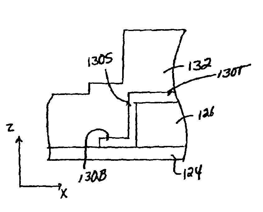
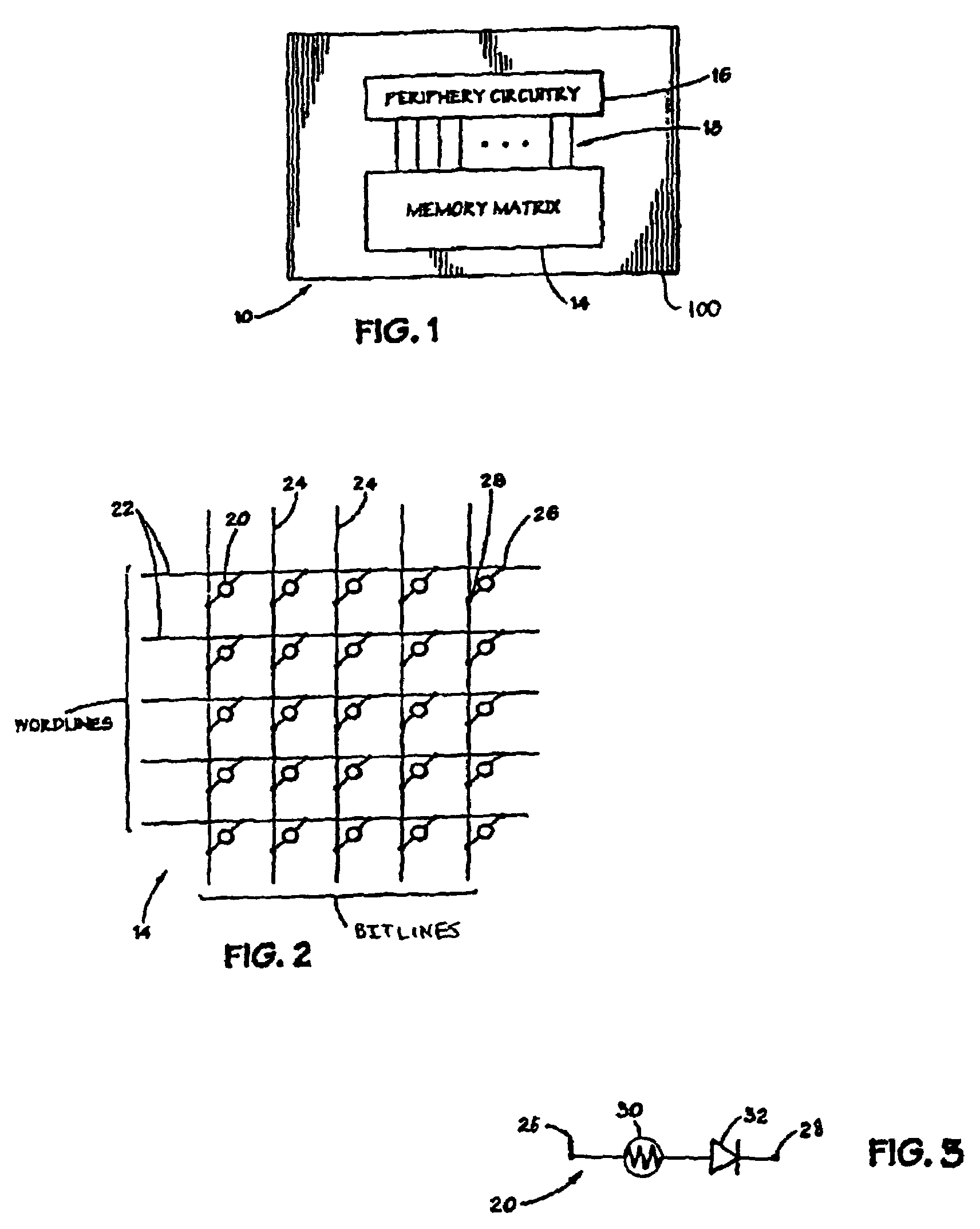
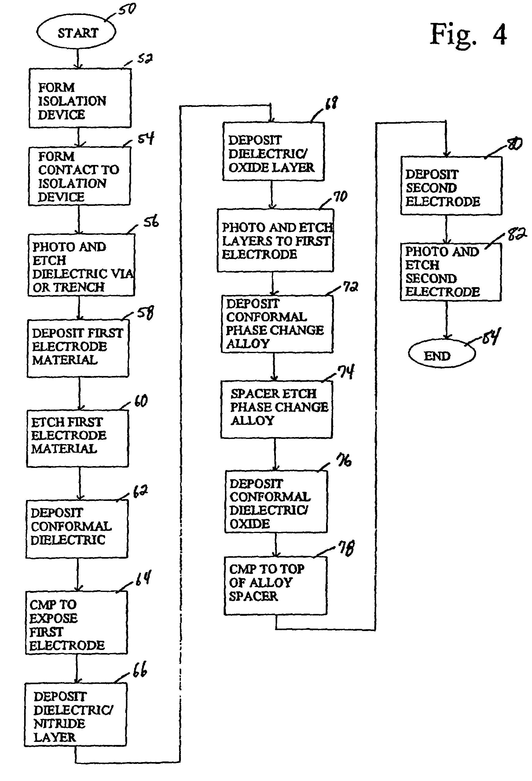
[0025]Programmable resistance memory elements comprise a volume of phase-change memory material that is programmable between at least a first resistance state and a second resistance state in response to programming electrical signals, such as currents, of different amplitudes and durations. Memory material programmable to two resistance states means that the associated memory element is capable of storing a single bit of information, either a logic 0 or a logic 1, for example. In another embodiment, the memory material is programmable to at least three resistance states so that each of the memory elements is capable of storing more than one bit of information. For example, memory material programmable to at least four resistance states makes a memory element capable of storing at least two bits of information. Each of the resistance states resulting from a programming electrical signal is assigned a value, such as logic 0 or logic 1 where two resistive states exist. Another electri...


PUM


Abstract

A programmable resistance memory element. The active volume of memory material is made small by the presence of a small area of contact between the conductive material and the memory material. The area of contact is created by forming a region of conductive material and an intersecting sidewall layer of the memory material. The region of conductive material is preferably a sidewall layer of conductive material.

Description

CROSS-REFERENCE TO RELATED APPLICATIONS[0001]This is a division of application Ser. No. 10 / 269,048, Filing Date Oct. 10, 2002 now abandoned, Applicant: Klersy, Patrick, title: PROGRAMMABLE RESISTANCE MEMORY ELEMENT AND METHOD FOR MAKING THE SAME, which was a continuation-in-part of U.S. patent application Ser. No. 09 / 276,273 filed on Mar. 25, 1999 now U.S. Pat. No. 6,969,866 which is a continuation-in-part of U.S. patent application Ser. No. 08 / 942,000, filed on Oct. 1, 1997 and now abandoned. U.S. patent application Ser. No. 09 / 276,273 is hereby incorporated by reference herein.FIELD OF INVENTION[0002]The present invention relates to memory elements and, more particularly, to programmable resistance memory elements.BACKGROUND OF THE INVENTION[0003]Memory elements formed from materials that can be programmed to exhibit at least two detectably distinct electrical resistivities are known in the art. One type of material that can be used as material for these programmable elements is p...

Claims


Application Information

Patent Timeline
Patent Type & Authority Patents(United States)
IPC IPC(8): H01L21/00G11C11/56H01L27/24H01L45/00
CPCG11C11/56G11C11/5678H01L27/2409H01L45/06H01L45/124H01L45/1273H01L45/144H01L45/1691G11C13/0004H10B63/20H10N70/8265H10N70/231H10N70/8418H10N70/8828H10N70/068
Inventor KLERSY, PATRICK
Owner OVONYX MEMORY TECH LLC
Why Eureka
Try Eureka