Stud bumps as local heat sinks during transient power operations

a technology of local heat sink and stud bump, which is applied in the direction of cooling/ventilation/heating modification, semiconductor/solid-state device details, semiconductor devices, etc., can solve the problems of not being populated or positioned, unsatisfactory options, and need to dissipate heat generated, so as to effectively dissipate heat and reduce junction temperature , the effect of dissipating hea

Active Publication Date: 2010-11-23
TEXAS INSTR INC
View PDF5 Cites 18 Cited by
  • Summary
  • Abstract
  • Description
  • Claims
  • Application Information

AI Technical Summary

Benefits of technology

[0005]Accordingly, a problem in high power IC devices is the need to dissipate heat generated during a transient (i.e. “ON”) function of the device. By effectively dissipating heat, a lower junction temperature can be maintained over longer “ON” periods.

Problems solved by technology

Accordingly, a problem in high power IC devices is the need to dissipate heat generated during a transient (i.e. “ON”) function of the device.
Although components of the IC devices do inherently dissipate heat, they can not be populated or positioned to the extent that they can effectively and consistently dissipate heat specifically at a hot spot.
Also, while it may be proposed to form a thicker copper layer over the die, such an option is unsatisfactory at least because the cost is relatively high and not specific to hot spots.
The thicker copper could be localized with a mask in fabrication, thereby reducing somewhat an amount of copper utilized, but this adds unnecessary steps.

Method used


Image

  • Stud bumps as local heat sinks during transient power operations
  • Stud bumps as local heat sinks during transient power operations
  • Stud bumps as local heat sinks during transient power operations

Examples


Embodiment Construction

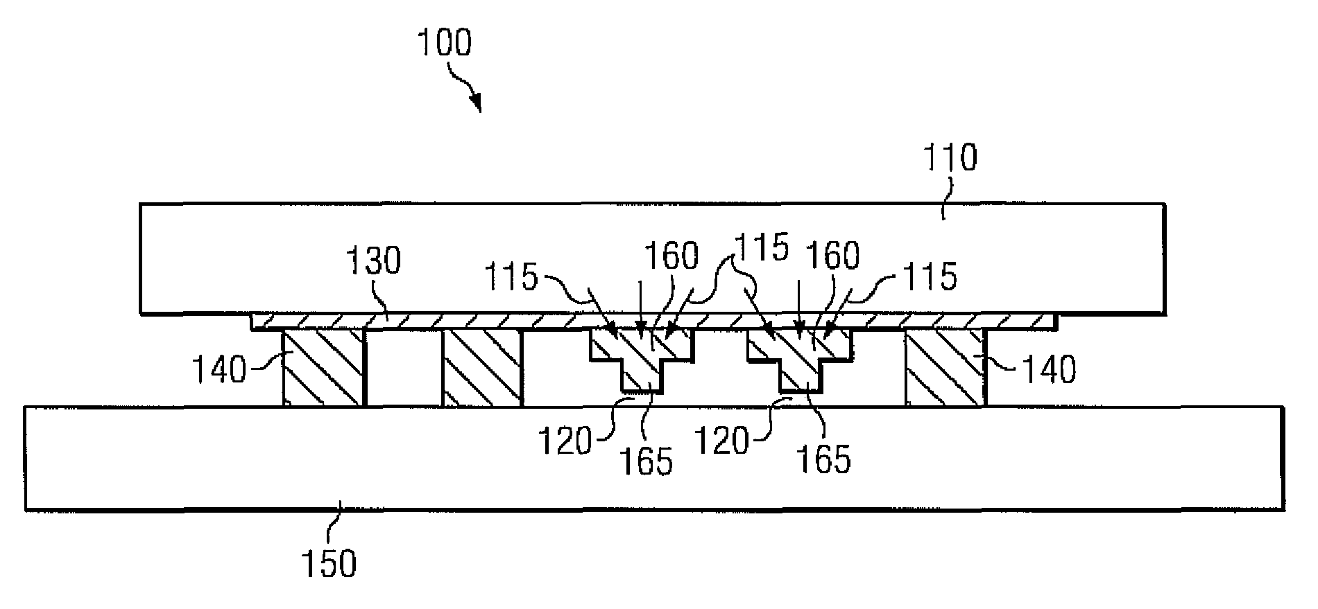
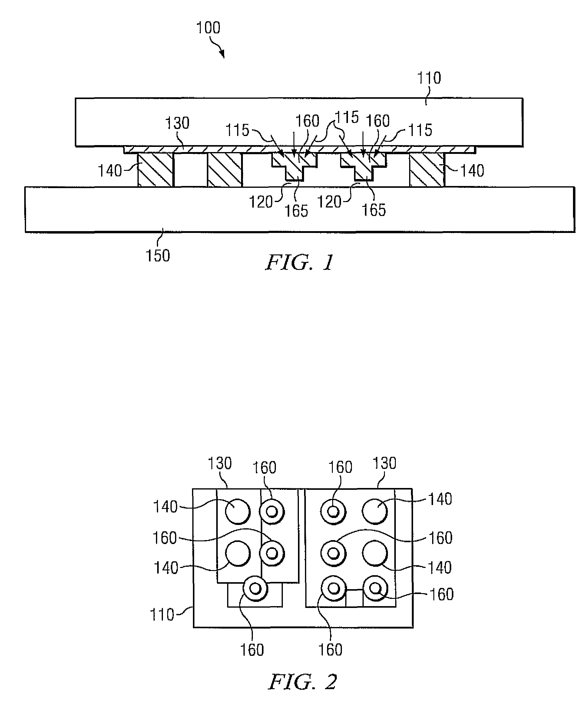
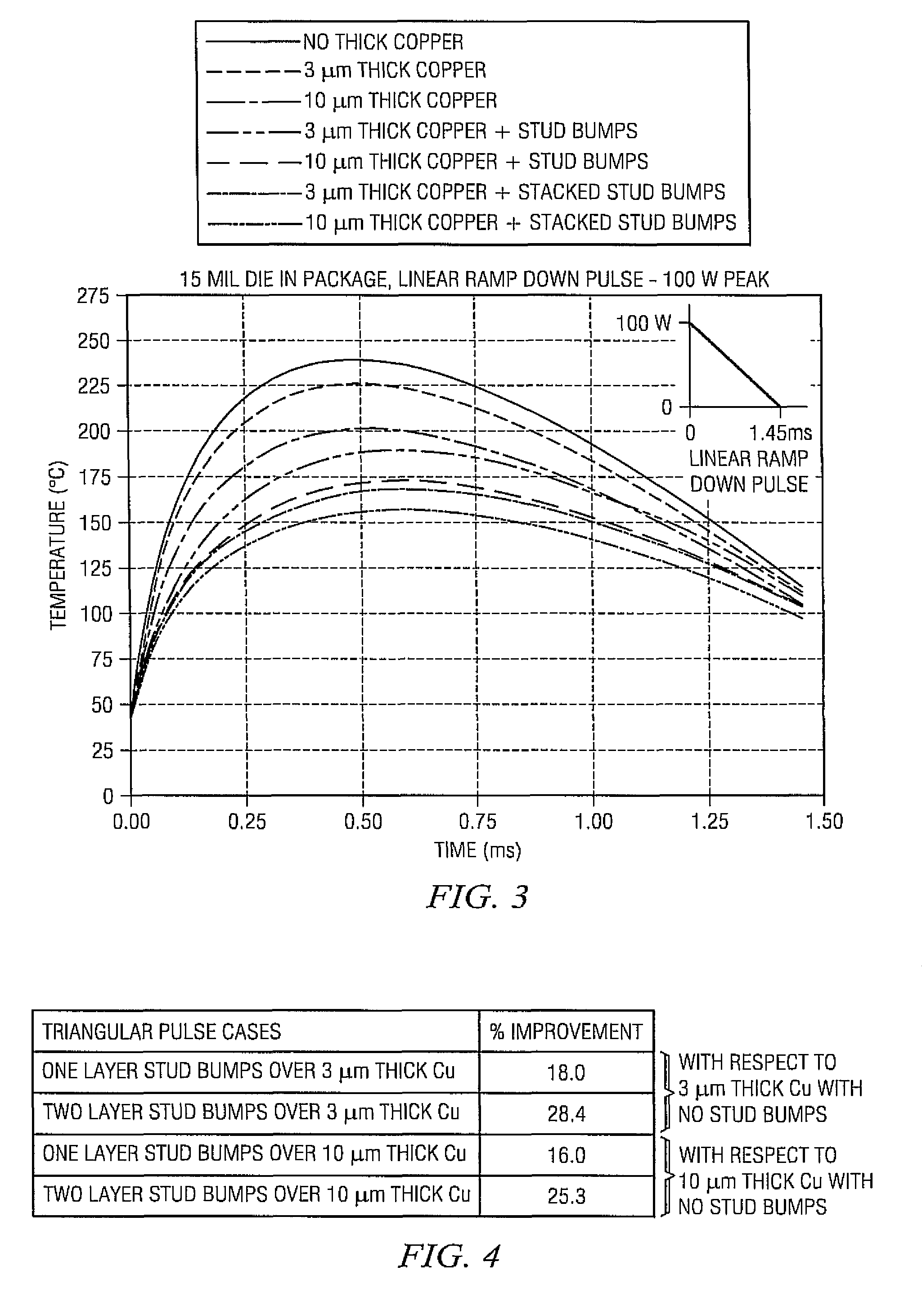
[0019]Reference will now be made in detail to the exemplary embodiments of the present disclosure, an example of which is illustrated in the accompanying drawings. Wherever possible, the same reference numbers will be used throughout the drawings to refer to the same or like parts.

[0020]In the following description, reference is made to the accompanying drawings that form a part thereof, and in which is shown by way of illustration specific exemplary embodiments which may be practiced. These embodiments are described in sufficient detail to enable those skilled in the art to practice the embodiments and it is to be understood that other embodiments may be utilized and that changes may be made without departing from the scope of the invention. The following description is, therefore, merely exemplary.

[0021]Notwithstanding that the numerical ranges and parameters setting forth the broad scope of the disclosure are approximations, the numerical values set forth in the specific examples...


PUM


Abstract

A thermal management configuration for a flip chip semiconductor device is disclosed. The device includes a high power silicon based die having a metal bonding surface. A plurality of interconnects are formed on the metal surface and connected to a substrate. A plurality of thermal management stud bumps are formed on the metal bonding surface, the thermal management stud bumps positioned distinct from the interconnects and local to die hot spots, exposed ends of the thermal management stud bumps spaced from the substrate.

Description

CROSS REFERENCE TO RELATED APPLICATIONS[0001]This application is a continuation-in-part of application Ser. No. 12 / 473,602, filed on May 28, 2009, and incorporated herein by reference, in its entirety.FIELD[0002]This invention relates generally to semiconductor thermal management, and more particularly placing and utilizing stud bumps as local heat sinks during transient power operations of a semiconductor device.BACKGROUND[0003]Heat dissipating structures have long been included in a variety of integrated circuit (IC) devices. Typical heat dissipating structures can be found in heat spreaders, cooling plates, Peltier devices, thermal adhesives, bonding over active circuits (BOAC) and use of varying structural materials in an effort to absorb and / or dissipate heat. In certain high power applications, an increase in temperature can adversely affect reliable device functioning.[0004]For example, high power semiconductor devices experience transient periods immediately after input powe...

Claims


Application Information

Patent Timeline
Patent Type & Authority Patents(United States)
IPC IPC(8): H01L23/10H01L23/12H01L23/34
CPCH01L23/3171H01L23/367H01L24/14H01L24/16H01L2224/16H01L2924/01079H01L2924/19041H01L2924/01084H01L2924/10253H01L2924/00H01L2224/0554H01L2224/05548H01L2224/05573H01L2224/056H01L2924/00014H01L2924/14H01L2224/05599H01L2224/0555H01L2224/0556
Inventor GURRUM, SIVA PRAKASHSAHASRABUDHE, KAPIL HERAMBGUPTA, VIKAS
Owner TEXAS INSTR INC
Why Eureka
Try Eureka