
Polishing device and substrate processing device

Inactive Publication Date: 2010-12-14
EBARA CORP
View PDF26 Cites 17 Cited by
  • Summary
  • Abstract
  • Description
  • Claims
  • Application Information

AI Technical Summary

Benefits of technology

[0006]The present invention has been made in view of the above drawback of the prior art. It is, therefore, an object of the present invention to provide a polishing apparatus which can reduce a space for the apparatus and can process and transfer a workpiece efficiently to improve throughput. Further, another object of the present invention is to provide a substrate processing apparatus which can reduce a space for the apparatus and can process and transfer a substrate efficiently to improve throughput.

Problems solved by technology

However, in the aforementioned polishing apparatus, since each polishing unit requires a pusher, a large space is required for installing the pushers.
Further, a large space is required for moving the transfer robot to transfer the wafer between the pushers, and thus the apparatus becomes larger.
Further, because the transfer robot cannot transfer a plurality of wafers at the same time, transfer of a target wafer may be delayed when the transfer robot is used to transfer another wafer in a case where the transfer robot is employed for various purposes.
In such a case, processing and transfer of wafers cannot be performed efficiently, so that throughput is lowered.

Method used


Image

  • Polishing device and substrate processing device
  • Polishing device and substrate processing device
  • Polishing device and substrate processing device

Examples


Embodiment Construction

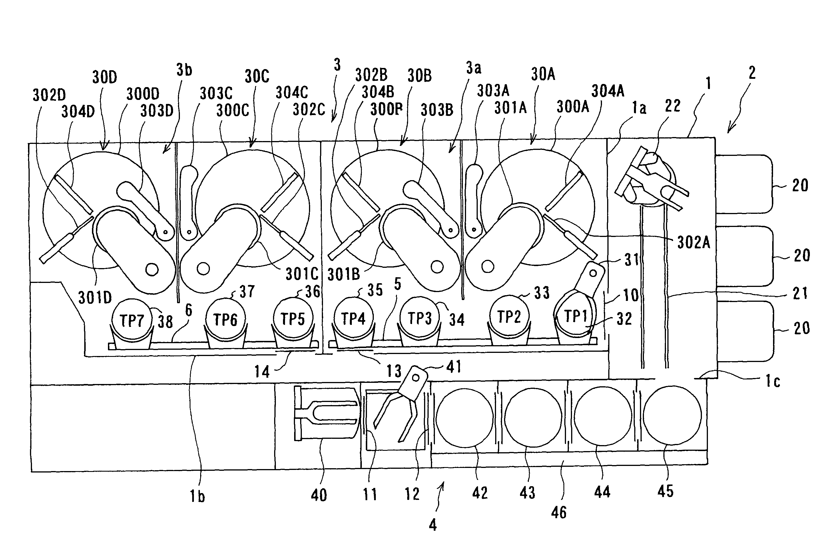
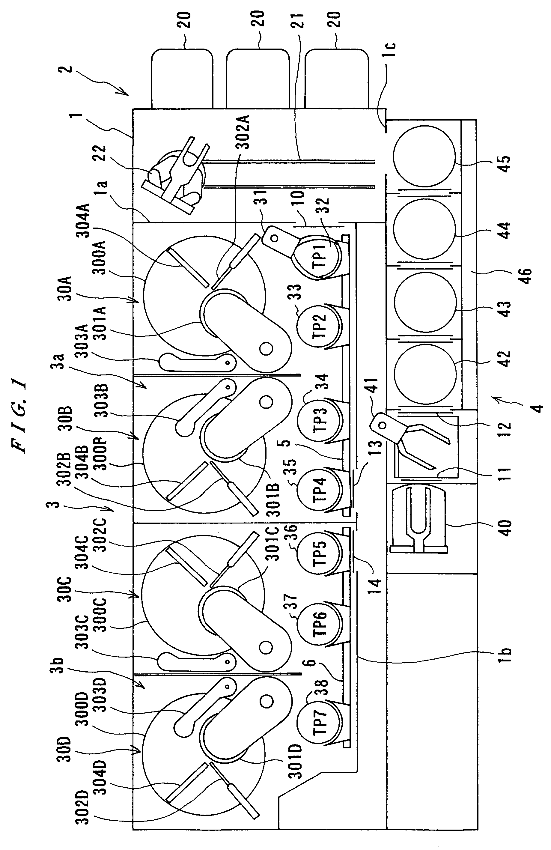
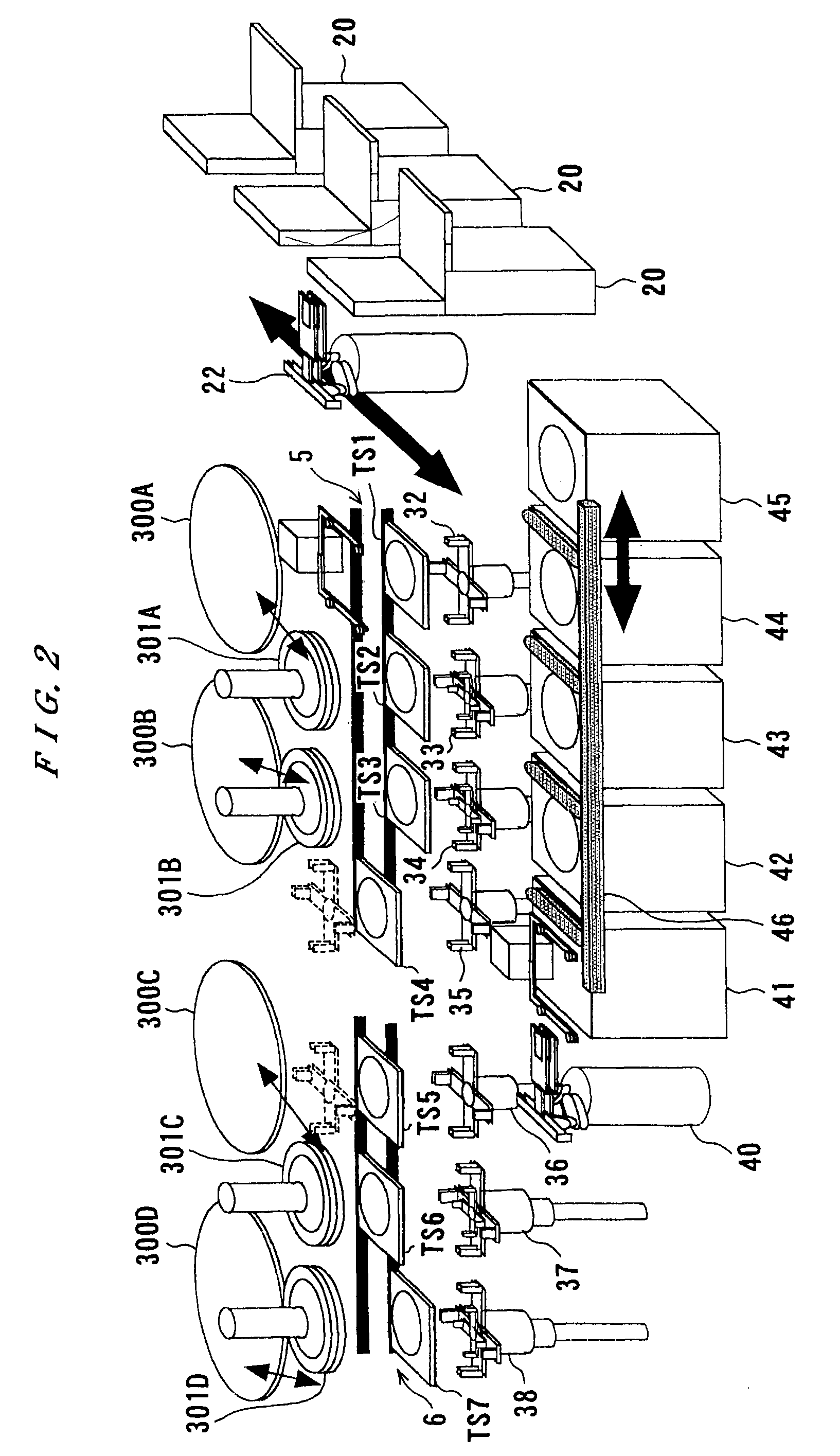
[0094]A polishing apparatus according to embodiments of the present invention will be described below in detail with reference to the accompanying drawings. FIG. 1 is a plan view showing an entire arrangement of a polishing apparatus according to an embodiment of the present invention, and FIG. 2 is a perspective view showing an outline of the polishing apparatus shown in FIG. 1. As shown in FIG. 1, the polishing apparatus in the present embodiment has a housing 1 in a rectangular form, and an interior of the housing 1 is divided into a loading / unloading section 2, a polishing section 3 (3a, 3b), and a cleaning section 4 by partition walls 1a, 1b, and 1c. The loading / unloading section 2, the polishing sections 3a, 3b, and the cleaning section 4 are assembled independently of each other, and air is discharged from these sections independently of each other.

[0095]The loading / unloading section 2 has at least two front loading portions 20 (three in the present embodiment) on which a waf...


PUM


Abstract

A polishing apparatus has a plurality of polishing units. Moving mechanisms for moving top rings between polishing positions on polishing surfaces and wafer receiving / delivering positions are provided in each of the polishing units. Linear transporters are provided for transferring a wafer between a plurality of transferring positions including the wafer receiving / delivering positions. Pushers for receiving and delivering the wafer between the linear transporters and the top rings are provided at the transferring positions as the wafer receiving / delivering positions.

Description

TECHNICAL FIELD[0001]The present invention relates to a substrate processing apparatus, and more particularly to a polishing apparatus for polishing a workpiece such as a semiconductor wafer to a flat mirror finish.BACKGROUND ART[0002]As semiconductor devices have become more highly integrated in recent years, circuit interconnections have become finer and distances between those interconnections have become smaller. In case of photolithography, which can form interconnections that are at most 0.5 μm wide, it is required that surfaces on which pattern images are to be focused by a stepper should be as flat as possible because a depth of focus of an optical system is relatively small. A polishing apparatus for performing chemical mechanical polishing (CMP) has been used as means for planarizing a surface of such a semiconductor wafer.[0003]This type of chemical mechanical polishing (CMP) apparatus comprises a polishing table having a polishing cloth thereon and a top ring. An abrasiv...

Claims


Application Information

Patent Timeline
IPC IPC(8): C23F1/00B24B37/04H01L21/00H01L21/304H01L21/677H01L21/68H01L21/687
CPCB24B37/345H01L21/67219H01L21/68707H01L21/67751H01L21/67766H01L21/67745H01L21/304H01L21/68
Inventor WAKABAYASHI, SATOSHITOGAWA, TETSUJIKOSUGE, RYUICHIATO, KOJISOTOZAKI, HIROSHI
Owner EBARA CORP
Features
  • Generate Ideas
  • Intellectual Property
  • Life Sciences
  • Materials
  • Tech Scout
  • Unparalleled Data Quality
  • Higher Quality Content
  • 60% Fewer Hallucinations
Learn More