Solder interconnect pads with current spreading layers

a technology of current spreading layer and solder interconnect, which is applied in the direction of semiconductor devices, semiconductor/solid-state device details, electrical apparatus, etc., can solve the problems of low resistance, complicated and limited performance of solder pads, and failure of electromigration void/high resistan

Inactive Publication Date: 2011-01-11
ULTRATECH INT INC
View PDF9 Cites 13 Cited by
  • Summary
  • Abstract
  • Description
  • Claims
  • Application Information

AI Technical Summary

Problems solved by technology

As the density of integrated circuits has increased and the dimensions of terminal pads has decreased, solder interconnect electromigration performance has become an issue.
Electromigration (the movement of metal in a wire, ultimately resulting in a void) performance of solder pads is complicated and limited by the interactive nature of conventional solder terminal structures and materials of such structures which form intermetallic compounds.
As more and intermetallics are formed, current density increases in the area of the intermetallics, leading to localized heating which increases intermetallic formation in an ever increasing cycle, ultimately resulting in electromigration void / high resistance failures.

Method used


Image

  • Solder interconnect pads with current spreading layers
  • Solder interconnect pads with current spreading layers
  • Solder interconnect pads with current spreading layers

Examples


Embodiment Construction

[0014]An intermetallic is defined as a solid phase compound containing two or more metallic elements, with optionally one or more non-metallic elements, whose structure is distinct from that of any of the constituents. Alloys, which are a homogeneous mixture of metals, and interstitial compounds such as carbides and nitrides are excluded under this definition. Examples of materials that form intermetallic compounds with tin include, but are not limited to copper, nickel, gold, platinum, antimony and palladium indium. Examples of materials that do not form intermetallic compounds with tin include, but are not limited to aluminum, titanium, tantalum and tungsten.

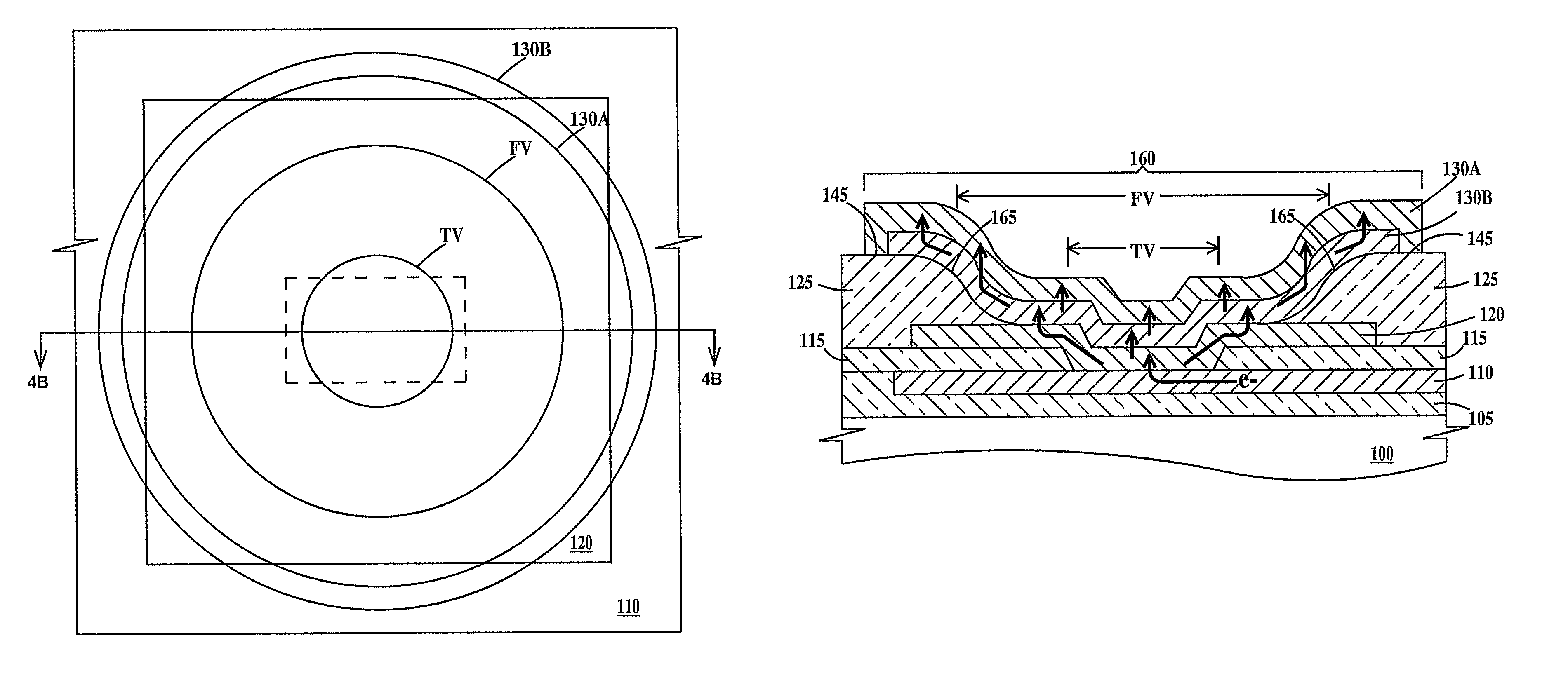
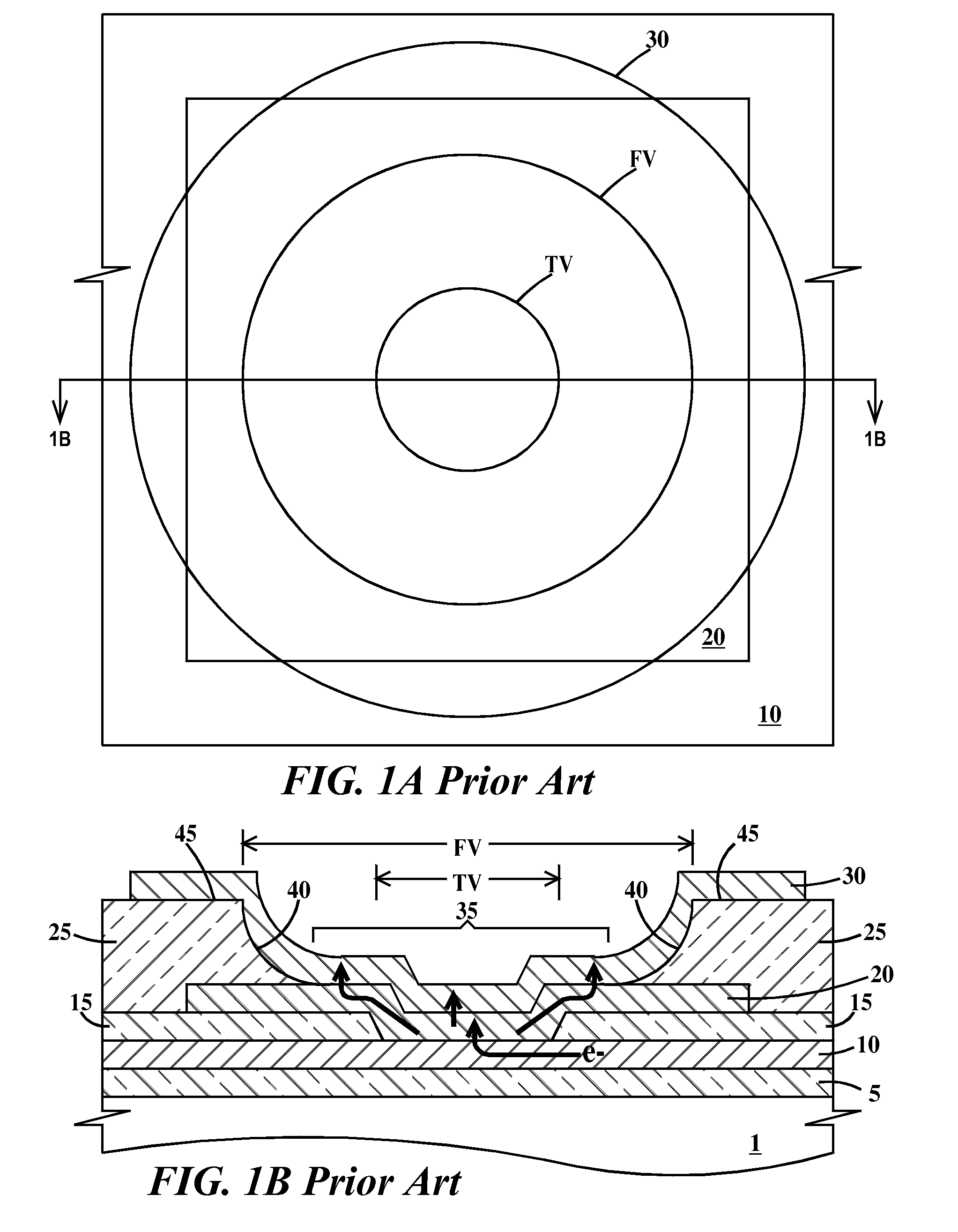
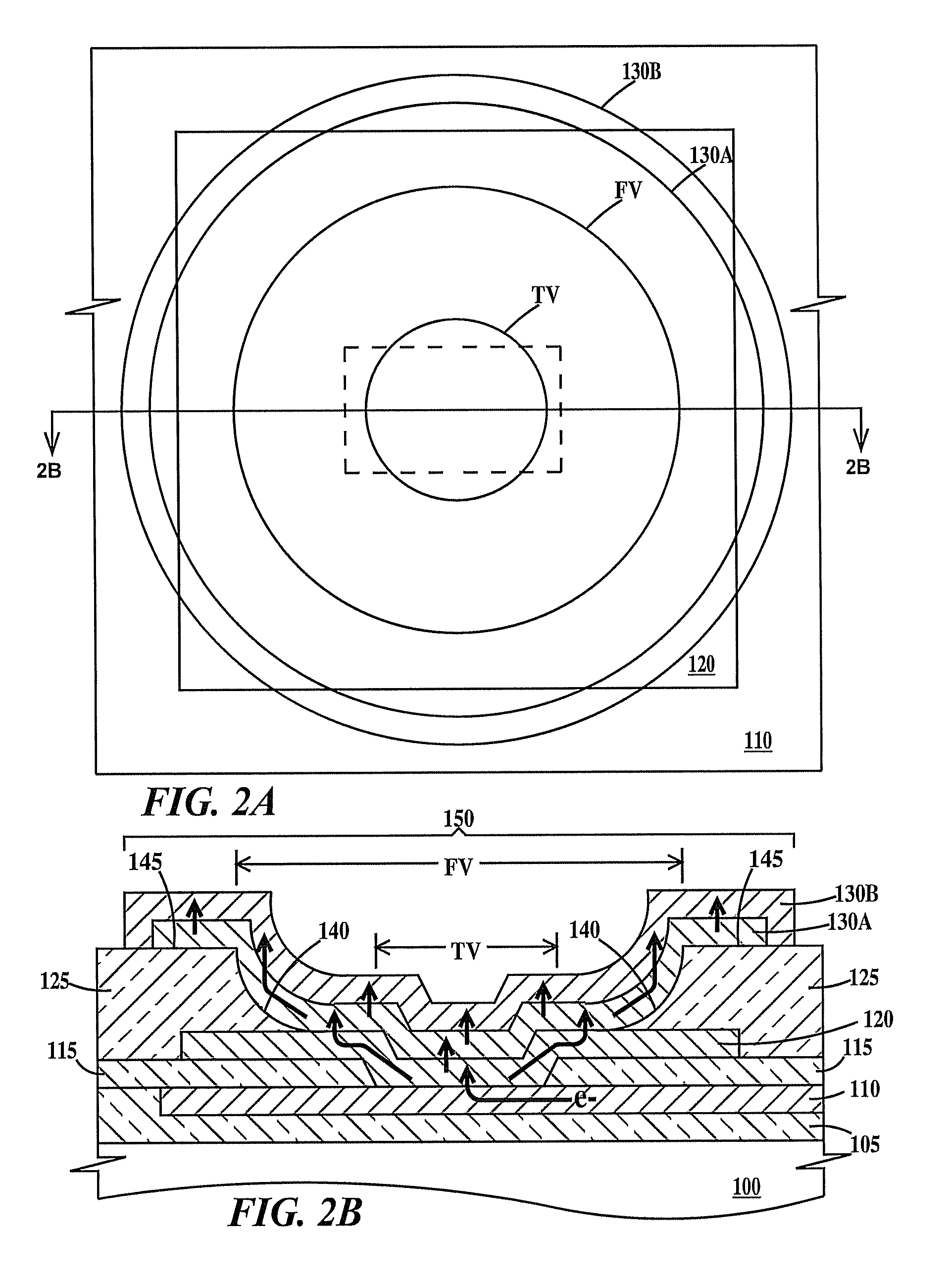
[0015]FIG. 1A is a plan view and FIG. 1B is a cross-section view through 1B-1B of FIG. 1A of a solder interconnect pad of the prior art. FIGS. 1A and 1B illustrate the problem solved by the embodiments of the present invention. In FIG. 1B, formed on a substrate 1 is a set (not fully shown) of interlevel dielectric layers conta...


PUM

PropertyMeasurementUnit
currentaaaaaaaaaa
thickaaaaaaaaaa
thickaaaaaaaaaa

Abstract

Structure and methods of making the structures. The structures include a structure, comprising: an organic dielectric passivation layer extending over a substrate; an electrically conductive current spreading pad on a top surface of the organic dielectric passivation layer; an electrically conductive solder bump pad comprising one or more layers on a top surface of the current spreading pad; and an electrically conductive solder bump containing tin, the solder bump on a top surface of the solder bump pad, the current spreading pad comprising one or more layers, at least one of the one or more layers consisting of a material that will not form an intermetallic with tin or at least one of the one or more layers is a material that is a diffusion barrier to tin and adjacent to the solder bump pad.

Description

FIELD OF THE INVENTION[0001]The present invention relates to the field of integrated circuits; more specifically, it relates to solder interconnect pads with a current spreader and methods of fabricating solder interconnect pads having current spreaders.BACKGROUND OF THE INVENTION[0002]As the density of integrated circuits has increased and the dimensions of terminal pads has decreased, solder interconnect electromigration performance has become an issue. Electromigration (the movement of metal in a wire, ultimately resulting in a void) performance of solder pads is complicated and limited by the interactive nature of conventional solder terminal structures and materials of such structures which form intermetallic compounds. For advanced technologies which use lead free solder materials with high tin contents, the electromigration lifetime (time to failure caused by electromigration) is directly dependent upon thermal process history as tin reacts with the metals used in the integra...

Claims


Application Information

Patent Timeline
Patent Type & Authority Patents(United States)
IPC IPC(8): H01L23/52
CPCH01L23/488H01L24/05H01L24/45H01L2924/01028H01L2224/05624H01L2224/13099H01L2224/16H01L2224/45147H01L2924/01013H01L2924/01014H01L2924/01018H01L2924/01022H01L2924/01027H01L2924/01029H01L2924/01046H01L2924/01049H01L2924/0105H01L2924/01051H01L2924/01073H01L2924/01074H01L2924/01078H01L2924/01079H01L2924/01082H01L2924/01327H01L2924/04941H01L2924/04953H01L2924/14H01L2924/19043H01L2224/0401H01L2924/0002H01L2224/05022H01L2224/05541H01L2224/05557H01L2224/13007H01L2924/01005H01L2924/01006H01L2924/01033H01L2924/01047H01L2924/014H01L2224/05572H01L2924/00014H01L24/13H01L2224/48824H01L2224/04042H01L2924/207H01L2924/00H01L2224/05552
Inventor DAUBENSPECK, TIMOTHY HARRISONSULLIVAN, TIMOTHY D.
Owner ULTRATECH INT INC
Why Eureka
Try Eureka