Layout design method of semiconductor integrated circuit having well supplied with potential different from substrate potential

a technology of integrated circuits and substrate potentials, applied in the direction of cad circuit design, computer aided design, transistors, etc., can solve the problems of increasing processes and design time, reducing the design standard, and difficulty in reducing the power consumption of semiconductor integrated circuits, so as to reduce the layout design time, improve the design quality, and facilitate chip design.

Active Publication Date: 2011-02-08
RENESAS ELECTRONICS CORP
View PDF26 Cites 2 Cited by
  • Summary
  • Abstract
  • Description
  • Claims
  • Application Information

AI Technical Summary

Benefits of technology

[0014]A layout design for a region separated from the substrate potential is achieved in the same process by using the second cell pattern. Thereby TAT (Turn around Time) for designing chips is reduced.
[0016]This enables to form the region separated from the substrate potential by just placing the second cell pattern stored in advance. Thereby chip design becomes easier and also design quality becomes improved.
[0017]The abovementioned configuration reduces layout design time and also improve layout design quality for achieving a high performance, downsized, and low power consuming semiconductor integrated circuit.

Problems solved by technology

Consequently it is difficult to reduce the power consumption of a semiconductor integrated circuit.
However separating a well potential in this way brings the following issue.
However, there is a latter mentioned problem in designing a semiconductor integrated circuit having a separating well region using a flow shown in FIG. 10.
The problem is that the method conducts a process of ST4 separately from a process of ST1 to ST3.
Further, an interval between basic cells placed in the substrate potential region and the separating well region inserted later may not satisfy a design standard.
This increases processes and design time.
Further, to insert a separating well region later, a design process of a semiconductor integrated circuit is complicated.
This will require a skilled designer and also could deteriorate design quality due to design error.

Method used


Image

  • Layout design method of semiconductor integrated circuit having well supplied with potential different from substrate potential
  • Layout design method of semiconductor integrated circuit having well supplied with potential different from substrate potential
  • Layout design method of semiconductor integrated circuit having well supplied with potential different from substrate potential

Examples


first embodiment

[0031]A preferred embodiment of the present invention is explained hereinafter in detail. The drawings are simplified as appropriate for clarity. Note that the same components are denoted by the same reference numerals and repetitive description will be omitted.

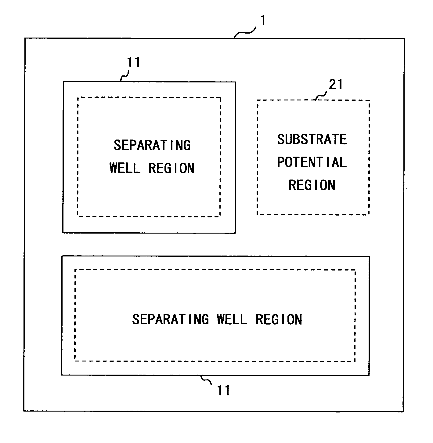
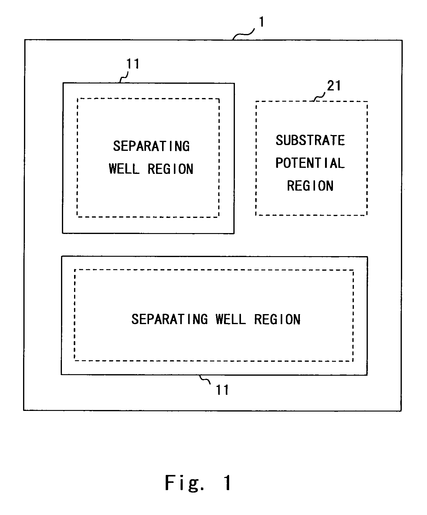
[0032]A first embodiment of the present invention is described hereinafter with reference to the drawings. FIG. 1 is a plan view showing a simplified layout of a semiconductor integrated circuit according to this embodiment. As shown in FIG. 1, a plurality of regions 11 that separates a substrate potential (hereinafter referred to as a separating well region 11) and a region 21 that does not separate the substrate potential (hereinafter referred to as a substrate potential region 21) are formed in a semiconductor integrated circuit 1.

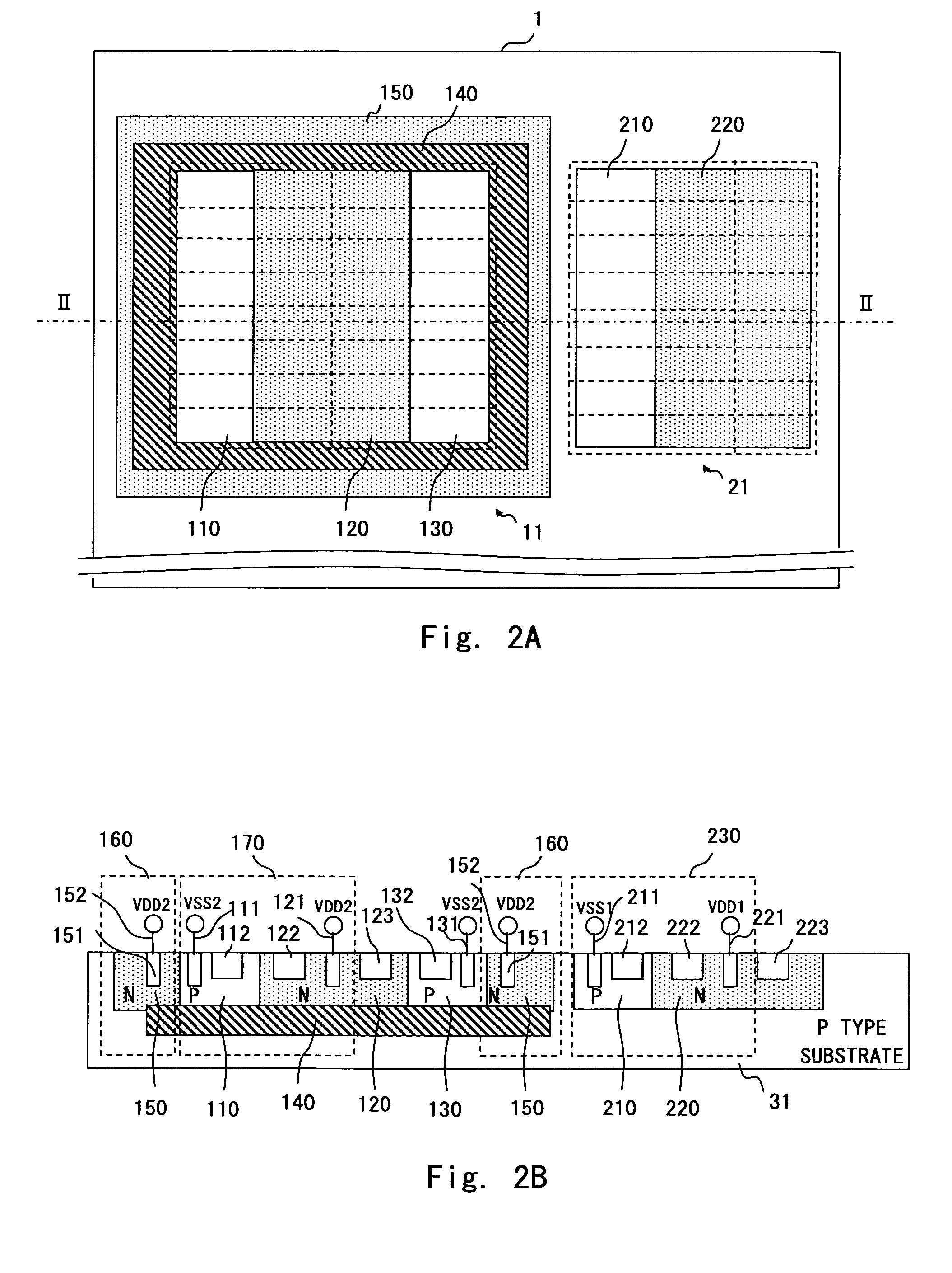
[0033]FIG. 2A is a schematic plan view showing the separating well region 11 and the substrate potential region 21. FIG. 2B is a cross-sectional diagram taken along the line II-II of FIG. 2A. As ...


PUM


Abstract

Design time (TAT) is reduced in a layout design of a semiconductor integrated circuit having a well supplied with a potential different from a substrate potential. A layout design method of the present invention includes preparing a first cell pattern placed on a semiconductor substrate of a first conductive type, preparing a second cell pattern having a deep well of a second conductive type, placing the first cell pattern in a first circuit region, and placing the second cell pattern in a second region different from the first circuit region. This reduces TAT in chip design.

Description

BACKGROUND OF THE INVENTION[0001]1. Field of the Invention[0002]The present invention relates to a layout design method of a semiconductor integrated circuit and a layout design tool of a semiconductor integrated circuit.[0003]2. Description of Related Art[0004]A demand for high performance, downsizing, and lower power consumption in a semiconductor integrated circuit including LSI (Large Scale Integration) which uses MOS (Metal Oxide Semiconductor) transistor has been increasing in recent years in order to achieve advanced data processing. However, a process technology for a semiconductor integrated circuit becomes narrower in order to achieve the high performance and the downsizing, a driving voltage for a semiconductor integrated circuit becomes lower. Accordingly a threshold voltage of a transistor decreases and a leak current in off state of a transistor increases. Consequently it is difficult to reduce the power consumption of a semiconductor integrated circuit.[0005]To resolv...

Claims


Application Information

Patent Timeline
Patent Type & Authority Patents(United States)
IPC IPC(8): H01L27/092H01L21/70H01L27/088H01L29/02H01L27/118
CPCG06F17/5068H01L27/0207H01L27/11807G06F30/39
Inventor YODA, KENICHI
Owner RENESAS ELECTRONICS CORP
Why Eureka
Try Eureka