Time-to-digital converter

a converter and time-to-digital technology, applied in the field of time-to-digital converters, can solve the problems of increasing the circuit scale and easy jitter in the path of the signal to be measured, and achieve the effects of reducing the circuit scale of the tdc circuit, high resolution and increasing time resolution

Inactive Publication Date: 2011-02-08
SEMICON TECH ACADEMIC RES CENT
View PDF9 Cites 22 Cited by
  • Summary
  • Abstract
  • Description
  • Claims
  • Application Information

AI Technical Summary

Benefits of technology

[0018]An object of the present invention is to solve the above-described problems and reduce the circuit scale of a TDC circuit with a high resolution.
[0019]In order to realize the above-mentioned object, in the time-to-digital converter (TDC) of the present invention, to the connection node or the input in the first stage of the first delay line in which first delay elements with a first delay amount are connected in series, one or more second delay elements with a second delay amount different from the first delay amount are connected in series, and a plurality of delayed clocks with a delay amount, which is an integer multiple of a unit delay amount, the unit delay amount being a difference between the first delay amount and the second delay amount, is generated successively, and as in the configuration in FIG. 1A, the relationship between the changing edges of the plurality of delayed clocks and a signal to be measured is detected with a plurality of judgment circuits (flip-flops) and an operation circuit (encoder circuit). If the first delay amount and the second delay amount are set so that the unit delay amount is small, the time resolution can be increased.
[0021]The conventional TDC shown in FIG. 2A requires two delay elements in order to generate a difference between the first delay amount and the second delay amount (unit delay amount). In contrast to this, according to the present invention, one delay element generates a unit delay amount, and therefore the number of delay elements can be halved and the circuit scale can be reduced.
[0026]According to the present invention, it is possible to realize a TDC circuit with a high resolution on a small circuit scale.

Problems solved by technology

With the vernier delay line TDC in FIG. 2A, resolution can be improved; however, there is a problem that the circuit scale is increased because the number of non-inverter buffers needs to be twice that of stages.
Because of this, there is a problem that jitter readily occurs in the path of the signal to be measured.

Method used


Image

  • Time-to-digital converter
  • Time-to-digital converter
  • Time-to-digital converter

Examples


Embodiment Construction

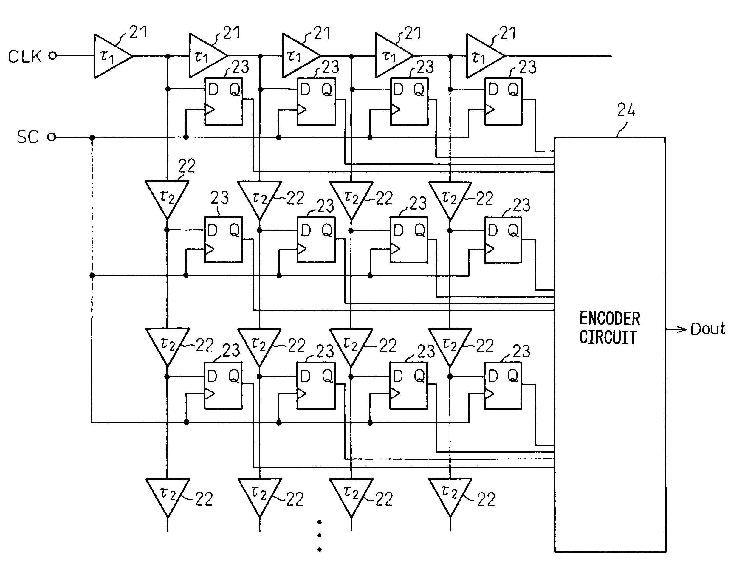
[0037]FIG. 3 is a diagram showing a basic configuration of a time-to-digital converter (TDC) of the present invention.

[0038]As shown in FIG. 3, a first delay line is provided, in which a plurality (five in the figure) of first delay elements (non-inverter buffers) 21 with delay amount τ1 is connected in series, and a reference clock CLK is input to the first stage. A second delay line, in which a plurality (three in the figure) of second delay elements (non-inverter buffers) 22 with a second delay amount τ2 is connected in series, is connected to each of the connection nodes (four in the figure) of first delay elements 21. The plurality (four in the figure) of the second delay lines is referred to as a second delay line group. In FIG. 3, the second delay line is not connected to the input node of the first delay element in the first stage of the first delay line; however, it is also possible to provide such a second delay line, as will be described later.

[0039]First delay element 21...


PUM


Abstract

A TDC circuit having a small scale circuit and high resolution is disclosed, which is a time-to-digital converter that detects a phase with respect to a reference clock of a signal to be measured, comprising a first delay line in which a plurality of first delay elements with a first delay amount is connected in series, a second delay line group that is connected to a plurality of connection nodes of the first delay line or an input node in the first stage and in which at least one or more second delay elements with a second delay amount different from the first delay amount are connected in series, a plurality of judgment circuits that judge whether the changing edge of the signal to be measured is advanced or delayed with respect to the changing edges of a delayed clock output from the first delay element and the second delay element, and an operation circuit that calculates a phase with respect to the reference clock of the changing edge of the signal to be measured from the judgment results, wherein a difference between the first delay amount and the second delay amount is smaller than the first delay amount and the second delay amount.

Description

BACKGROUND OF THE INVENTION[0001]1. Field of the Invention[0002]The present invention relates to a time-to-digital converter (TDC), and more specifically, to a TDC having a small circuit scale and high resolution.[0003]2. Related Art[0004]Recently, the performance of AD converters has improved remarkably and there is a demand for the detection of the accuracy of control signals that serve as a reference for operation, for example, the detection of jitters and periodic errors, with high precision. As a circuit to detect phase (jitter) with respect to the reference clock of a signal to be measured, which is a control signal, a TDC is widely known.[0005]FIG. 1A is a diagram showing a basic circuit configuration of a conventional TDC and FIG. 1B is a time chart showing the circuit operation of the conventional TDC in FIG. 1A.[0006]As shown in FIG. 1A, the TDC has a delay circuit line (delay line), in which a plurality of delay elements (non-inverter buffers) 11 that sequentially delay a...

Claims


Application Information

Patent Timeline
Patent Type & Authority Patents(United States)
IPC IPC(8): H03M1/50
CPCG04F10/06
Inventor SHIMIZU, KAZUYAKANETA, MASATOKOBAYASHI, HARUOMATSUURA, TATSUJIYAGI, KATSUYOSHIABE, AKIRAMASHIKO, KOICHIRO
Owner SEMICON TECH ACADEMIC RES CENT
Why Eureka
Try Eureka