Active pixel sensor with coupled gate transfer transistor

a technology of coupled gate transfer transistor and active pixel sensor, which is applied in the field of active pixel sensor, can solve the problems of low manufacturing cost and power consumption, disadvantages in noise and image quality, and difficulty in raising the initial potential of floating diffusion node b>120/b> beyond a given potential level, so as to improve the dynamic range of light signals and reduce image lag

Active Publication Date: 2011-02-15
SAMSUNG ELECTRONICS CO LTD
View PDF9 Cites 5 Cited by
  • Summary
  • Abstract
  • Description
  • Claims
  • Application Information

AI Technical Summary

Benefits of technology

[0022]Exemplary embodiments of the present disclosure provide an active pixel sensor having an improved dynamic range of light signals and reduced image lag.
[0023]Other exemplary embodiments of the present disclosure provide an active pixel sensor array with a shared structure using the active pixel sensors having an improved dynamic range of light signals and reduced image lag.
[0024]Still other exemplary embodiments of the present disclosure provide an active pixel sensor adopting a multi-layer photodiode structure having an improved dynamic range of light signals and reduced image lag.

Problems solved by technology

The CCD type generally has lower noise levels and better image quality than the CMOS type, but has disadvantages in manufacturing costs and power consumption.
The CMOS type, however, is disadvantageous in terms of noise and image quality, due to a low signal-to-noise ratio (SNR) and a narrow signal dynamic range.
However, when a power supply having a limited voltage level is used, it is difficult to raise the initial potential of the floating diffusion node 120 beyond a given potential level.
Failure to empty all photoelectrons within the photodiode at one sensing operation causes an image lag.
However, when power supplies having limited voltage levels are used, it is still difficult to raise the initial potential of the floating diffusion node 120 beyond the given potential level.

Method used


Image

  • Active pixel sensor with coupled gate transfer transistor
  • Active pixel sensor with coupled gate transfer transistor
  • Active pixel sensor with coupled gate transfer transistor

Examples


Embodiment Construction

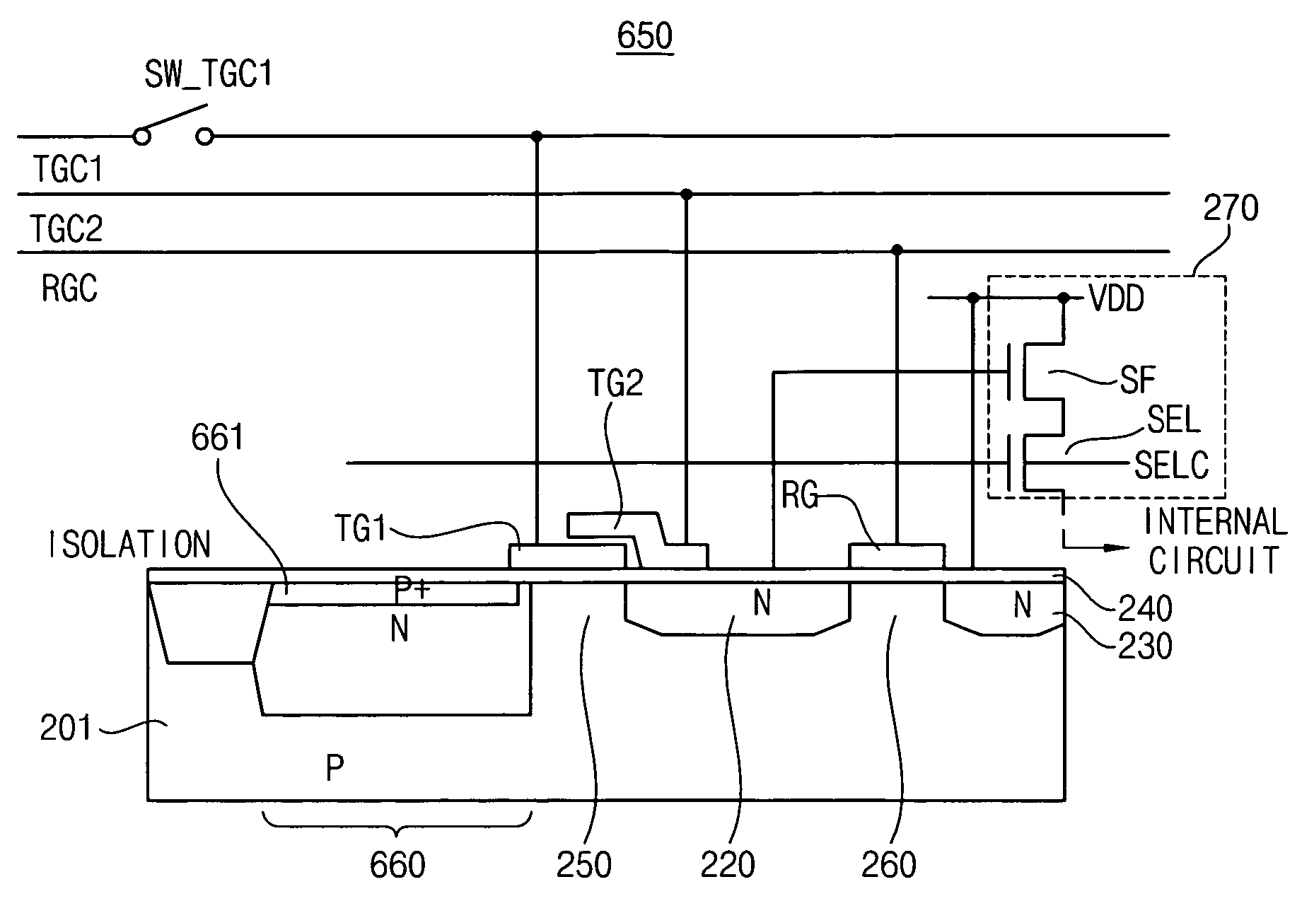
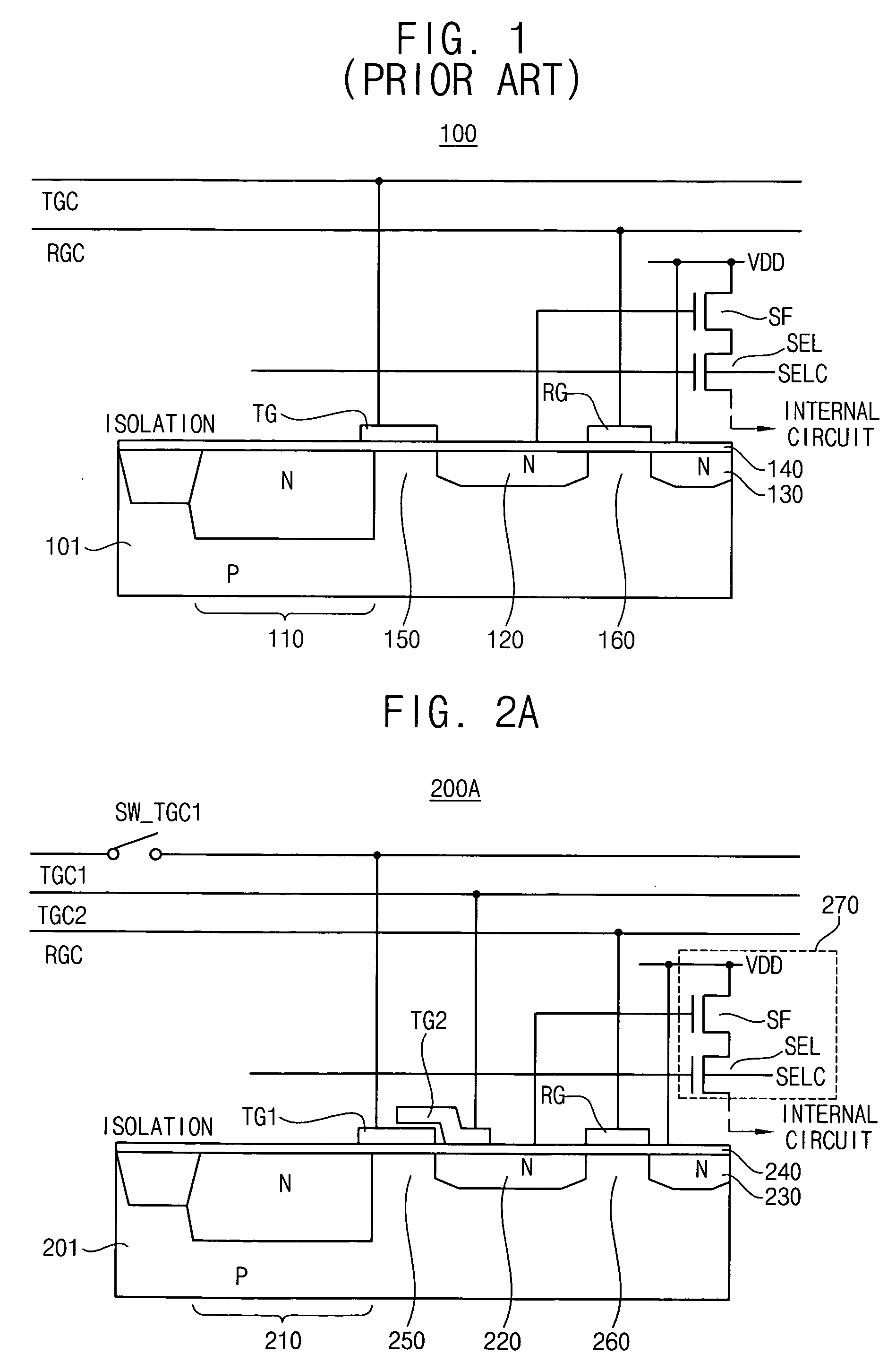
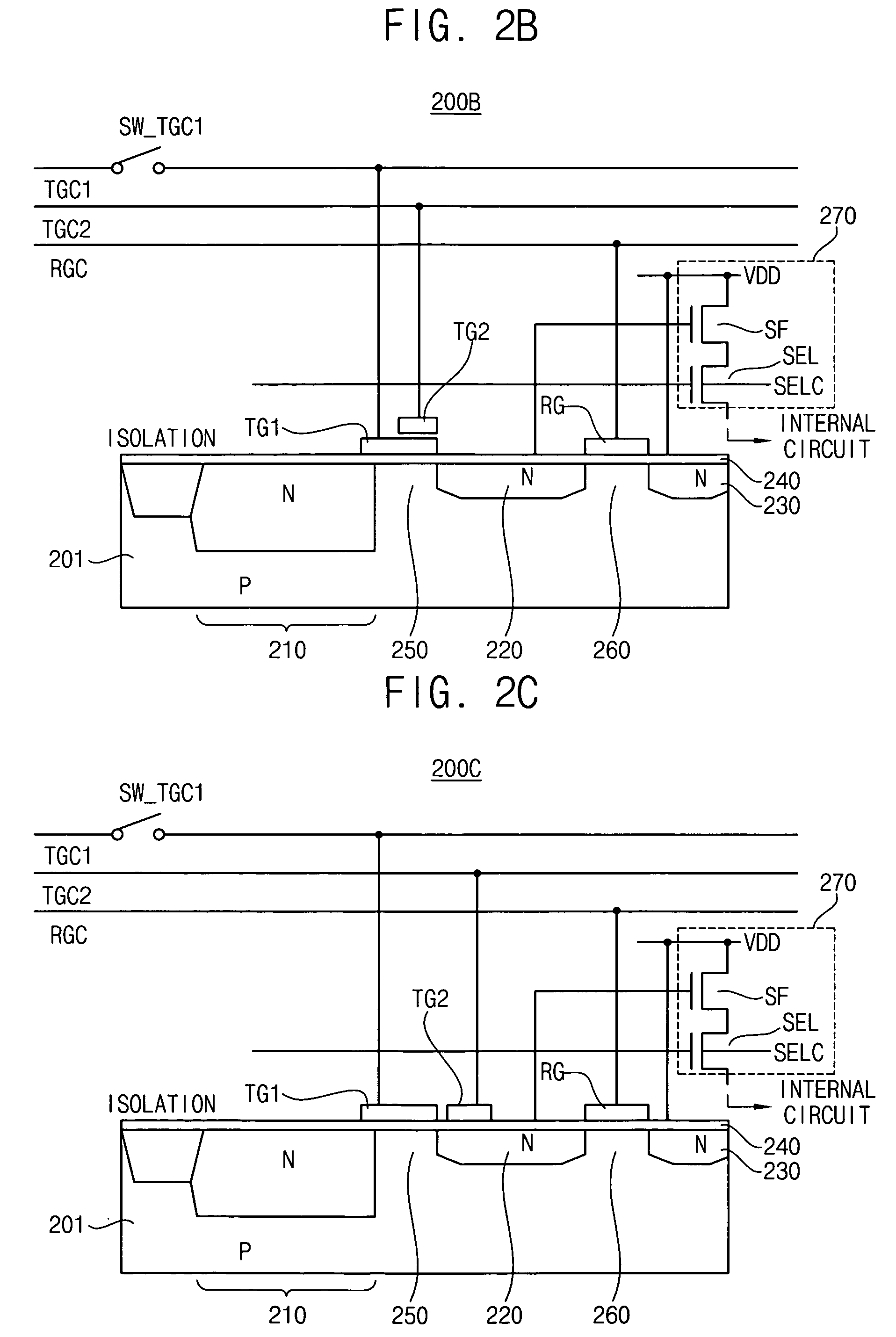
[0049]The invention is described more fully hereinafter with reference to the accompanying drawings, in which exemplary embodiments of the invention are shown. This invention may, however, be embodied in many different forms and should not be construed as limited to the embodiments set forth herein. Rather, these embodiments are provided so that this disclosure will be thorough and complete, and will convey the scope of the invention to those skilled in the art. In the drawings, the size and relative sizes of layers and regions may be exaggerated for clarity.

[0050]It will be understood that when an element or layer is referred to as being “on”, “connected to” or “coupled to” another element or layer, it can be directly on, connected or coupled to the other element or layer or intervening elements or layers may be present. In contrast, when an element is referred to as being “directly on,”“directly connected to” or “directly coupled to” another element or layer, there are no interven...


PUM


Abstract

A complementary metal-oxide semiconductor (CMOS) active pixel sensor includes a photodiode, a transfer transistor with a coupled gate, a reset transistor and a signal transfer circuit, where the photodiode generates electric charges in response to incident light, the transfer transistor transfers the electric charges integrated in the photodiode to a floating diffusion node, wherein the transfer transistor has a first transfer gate and a second transfer gate, and the first and second transfer gates have a coupled gate structure, the reset transistor resets a potential level of the floating diffusion node by a given voltage level, the signal transfer circuit transfers the potential level of the floating diffusion node to an internal circuit in response to a selection signal, and the CMOS active pixel sensor with the coupled gate may increase a capacity of the photodiode and reduce an image lag by using a voltage coupling effect of the coupled gate.

Description

CROSS-REFERENCE TO RELATED APPLICATION[0001]This application claims the benefit under 35 U.S.C. §119 of Korean Patent Application No. 2004-111655, filed on Dec. 24, 2004, which is herein incorporated by reference in its entirety.BACKGROUND OF THE INVENTION[0002]1. Field of the Invention[0003]The present disclosure relates to active pixel sensors, and more particularly relates to metal-oxide semiconductor active pixel sensors.[0004]2. Description of the Related Art[0005]Active pixel sensors (APS) convert photo images into electric signals, and are widely used in digital cameras, mobile phones with built-in cameras, monitoring systems, and the like.[0006]Presently, active pixel sensors are roughly classified as a type of charge coupled device (CCD) and a type of complementary metal-oxide semiconductor (CMOS). The CCD type generally has lower noise levels and better image quality than the CMOS type, but has disadvantages in manufacturing costs and power consumption. The APS of the CMOS...

Claims


Application Information

Patent Timeline
Patent Type & Authority Patents(United States)
IPC IPC(8): H01L27/144H01L27/146H04N5/335H04N5/355H04N5/369H04N5/374H04N5/3745H04N5/376
CPCH01L27/14603H01L27/14643H01L27/14647H04N3/155H01L27/14621H04N25/59H04N25/778H04N25/77H01L27/146H01L31/10
Inventor AHN, JUNG-CHAKASABA, TETSUOKIM, YOUNG-CHAN
Owner SAMSUNG ELECTRONICS CO LTD
Why Eureka
Try Eureka