Nonvolatile semiconductor memory and data programming/erasing method

a nonvolatile semiconductor and data programming technology, applied in semiconductor devices, digital storage, instruments, etc., can solve the problems of increasing current consumption and increasing element size, and achieve the effect of reducing element size, improving electron injection efficiency, and reducing applied voltag

Active Publication Date: 2011-02-15
RENESAS ELECTRONICS CORP
View PDF15 Cites 2 Cited by
  • Summary
  • Abstract
  • Description
  • Claims
  • Application Information

AI Technical Summary

Benefits of technology

[0017]In the case of the FN tunneling by the use of the electric field concentration, an efficiency of the electron injection is improved as compared with the conventional FN tunneling. Therefore, the applied voltage can be designed to be smaller. To put it the other way around, the electron injection can be well achieved even if the applied voltage is set to be comparatively small, because the electric field concentration is generated. When the applied voltage is reduced, the breakdown voltage required for the memory cell transistor also becomes smaller, which can reduce the element size. In other words, according to the present invention, the increase in the element size is suppressed although the FN tunneling method is adopted.
[0018]Moreover, according to the present invention, the CHE method is not adopted for the electron injection. Instead, the FN tunneling method is adopted for the electron injection. Therefore, the current consumption is reduced as compared with the case where the CHE method is used.
[0019]According to the present invention, as described above, it is possible in the charge trapping memory to reduce the current consumption with suppressing the increase in the element size.

Problems solved by technology

This causes increase in the element size.
As described above, the CHE method requires a large amount of current, which leads to increase in current consumption.

Method used


Image

  • Nonvolatile semiconductor memory and data programming/erasing method
  • Nonvolatile semiconductor memory and data programming/erasing method
  • Nonvolatile semiconductor memory and data programming/erasing method

Examples


first embodiment

1. First Embodiment

[0058]1-1. Cell Structure

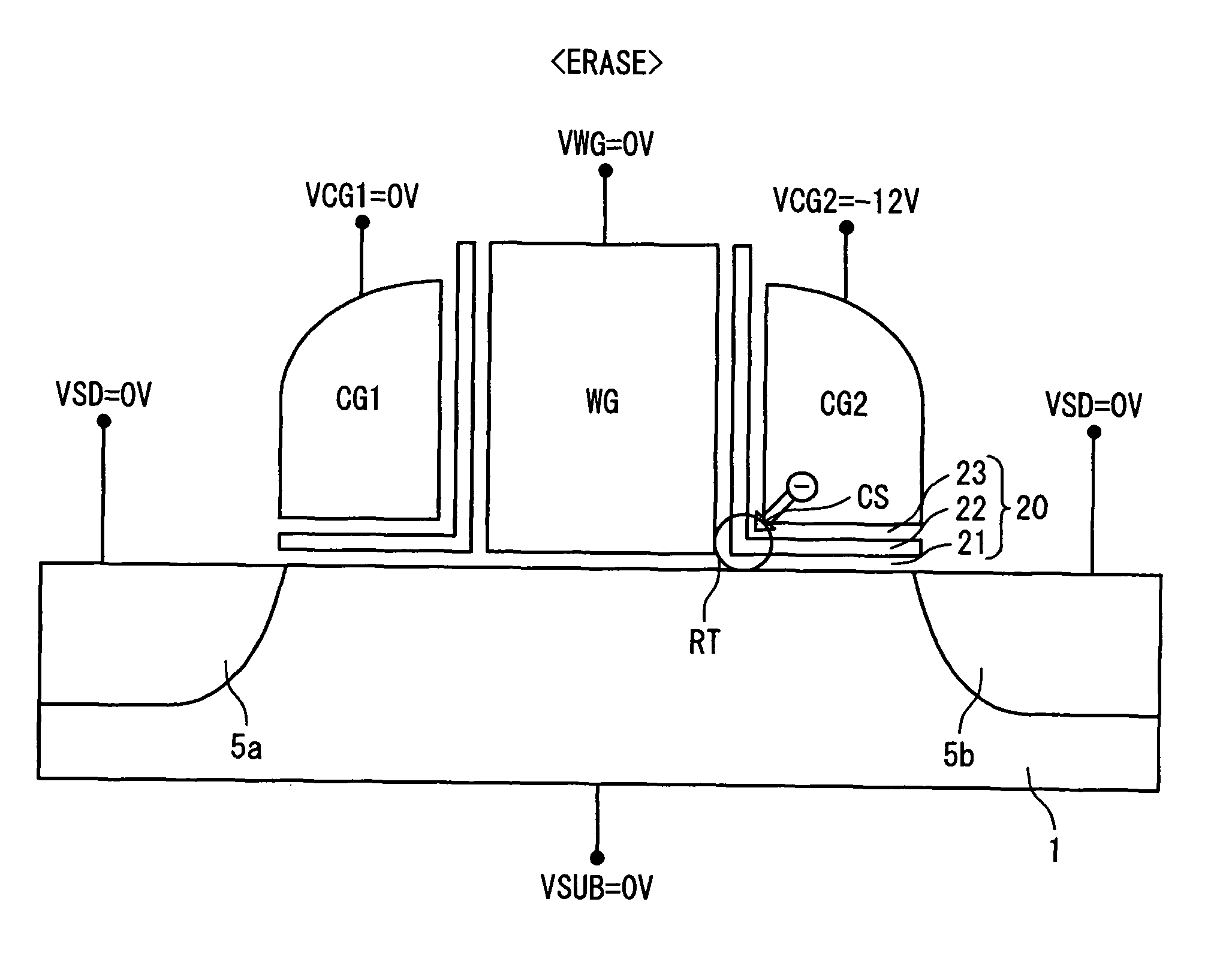
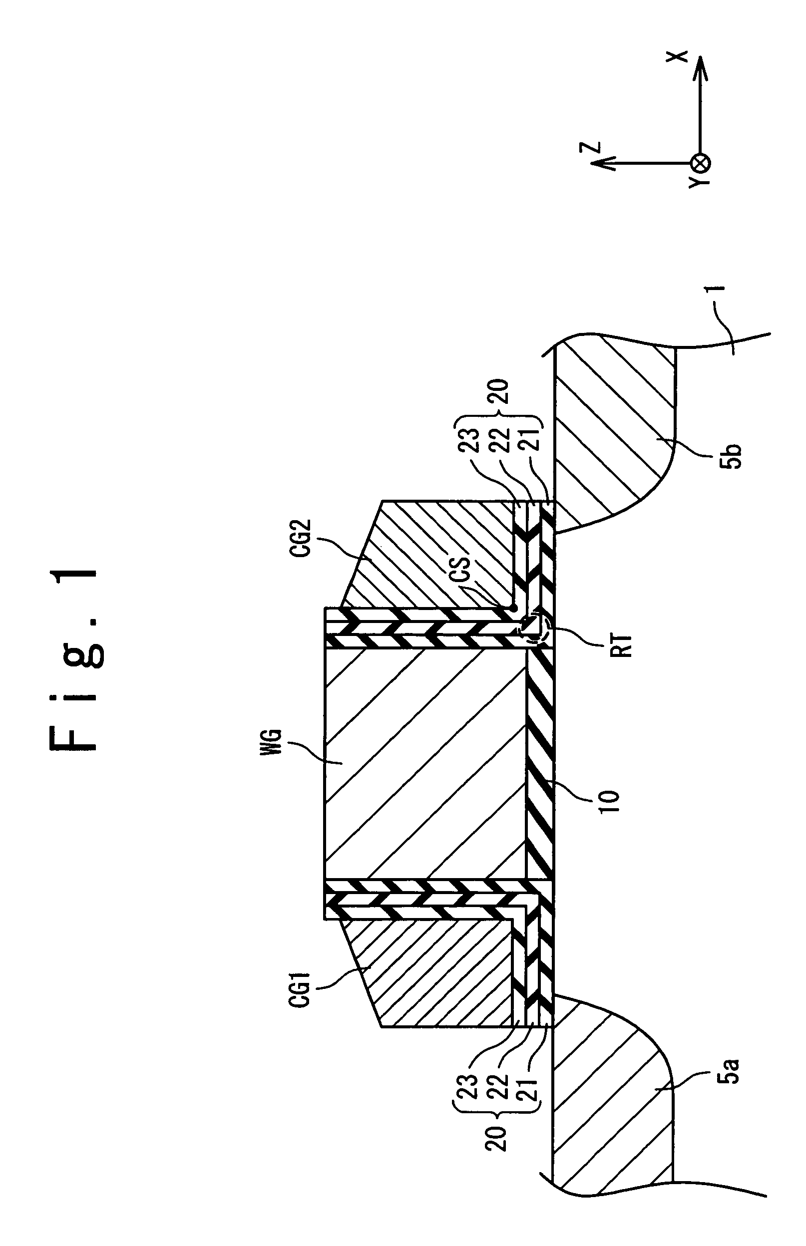
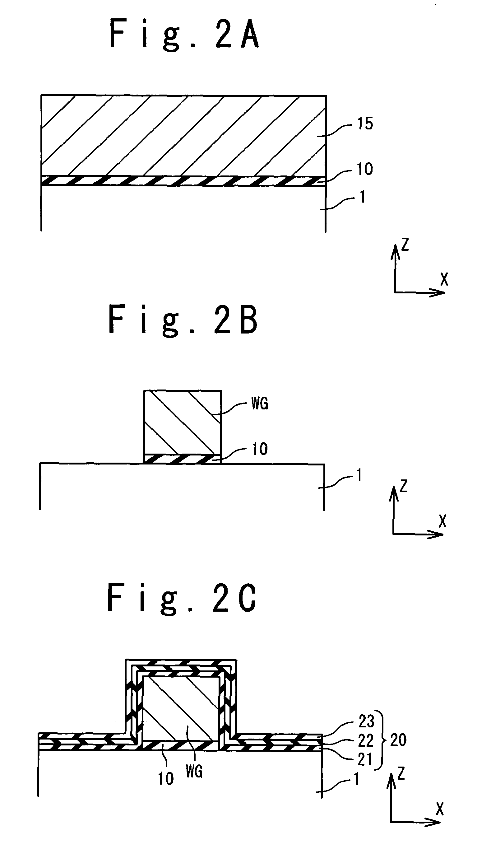
[0059]FIG. 1 is a cross-sectional view showing a structure of a nonvolatile semiconductor memory according to a first embodiment. In particular, FIG. 1 shows a cross-sectional structure of a memory cell transistor. The memory cell transistor according to the present embodiment will be described below with reference to FIG. 1.

[0060]Diffusion regions 5a and 5b which serve as source / drain are formed in a semiconductor substrate 1. For example, the semiconductor substrate 1 is a P-type silicon substrate (P-type well) and the diffusion regions 5a and 5b are N-type diffusion regions. A semiconductor region between the diffusion regions 5a and 5b is a channel region and the channel direction is the X-direction. A plurality of gate electrodes (WG, CG1, CG2) are provided over the channel region. The gate electrodes (WG, CG1, CG2) extend in the Y-direction perpendicular to the X-direction.

[0061]More specifically, the plurality of gate electrodes are...

second embodiment

2. Second Embodiment

[0128]FIG. 15 is a cross-sectional view showing a structure of a nonvolatile semiconductor memory according to a second embodiment. An overlapping description with the first embodiment will be omitted as appropriate.

[0129]In the second embodiment, the side surfaces of the word gate WG and the control gate CG are formed in a tapered shape. More specifically, an angle θ of the edge section CS of the control gate CG can be defined in the YZ-plane, as shown in FIG. 15. The angle θ can also be defined as an angle between a bottom surface of the control gate CG and a side surface of the control gate CG facing the word gate WG. The angle θ has been about 90 degrees in the first embodiment. In the second embodiment, the angle θ is less than 90 degrees. As the angle θ becomes smaller, the electric field becomes more and more convergent to the edge section CS, namely, the electric field concentration is further intensified. From a viewpoint of the electric field concentrat...

third embodiment

3. Third Embodiment

[0133]FIG. 17 is a cross-sectional view showing a structure of a nonvolatile semiconductor memory according to a third embodiment. An overlapping description with the first embodiment will be omitted as appropriate.

[0134]In the third embodiment, a step is formed on the surface of the semiconductor substrate 1. In other words, the surface of the semiconductor substrate 1 has an upper stage SU and a lower stage SL which form the step. The word gate WG is formed on the upper stage SU through the first gate insulating film 10. On the other hand, the control gate CG is formed on the lower stage SL through the second gate insulating film 20. As a result, a channel length around the trap region RT trapping electrons increases by ΔL as compared with the first embodiment. Since the channel length around the trap region RT increases, an OFF current of the memory cell transistor is further reduced. That is, an effect that the OFF current is further reduced can be obtained in...


PUM


Abstract

A nonvolatile semiconductor memory comprises: a semiconductor substrate; a first gate electrode formed on a surface of the semiconductor substrate through a first gate insulating film; a second gate electrode formed on the surface of the semiconductor substrate through a second gate insulating film and being adjacent to the first gate electrode through an insulating film; a charge trapping film formed at least in a trap region surrounded by the semiconductor substrate, the first gate electrode and the second gate electrode; and a tunnel insulating film formed between the charge trapping film and the second gate electrode. In one of programming and erasing, electrons are injected into the charge trapping film from the second gate electrode through the tunnel insulating film by Fowler-Nordheim tunneling.

Description

INCORPORATION BY REFERENCE[0001]This application is based upon and claims the benefit of priority from Japanese patent application No. 2007-272928, filed on Oct. 19, 2007, the disclosure of which is incorporated herein in its entirely by reference.BACKGROUND OF THE INVENTION[0002]1. Field of the Invention[0003]The present invention relates to a nonvolatile semiconductor memory. In particular, the present invention relates to a charge-trapping type nonvolatile semiconductor memory and a data programming / erasing method for the charge-trapping type nonvolatile semiconductor memory.[0004]2. Description of Related Art[0005]A flash memory and a charge trapping memory are known as an electrically erasable and programmable nonvolatile semiconductor memory. The charge trapping memory among them stores data by using an element that can trap charges. For example, the element for trapping charges is a MONOS (Metal Oxide Nitride Oxide Silicon) transistor. The MONOS transistor is a kind of a MIS ...

Claims


Application Information

Patent Timeline
Patent Type & Authority Patents(United States)
IPC IPC(8): G11C16/04
CPCG11C16/0425G11C16/10H01L21/28282H01L29/42344H01L29/42352H01L29/7923H01L29/40117
Inventor SAITOU, TOMOYA
Owner RENESAS ELECTRONICS CORP
Why Eureka
Try Eureka