Electronic circuit, electro-optical device, and electronic apparatus including the same

a technology of electrooptical devices and electronic devices, applied in the direction of optical radiation measurement, radiation control devices, instruments, etc., can solve the problems of reducing the dynamic range where a/d conversion is possible, poor saturation characteristics of polysilicon thin-film transistors, and reducing the flexibility of sensor arrangement, so as to improve the freedom of sensor arrangement and display quality. , the effect of reducing the cos

Active Publication Date: 2011-02-22
JAPAN DISPLAY WEST
View PDF17 Cites 7 Cited by
  • Summary
  • Abstract
  • Description
  • Claims
  • Application Information

AI Technical Summary

Benefits of technology

[0037]An advantage of some aspects of the invention is that an A / D conversion circuit including polysilicon thin-film transistors is provided in which a sufficient A / D conversion dynamic range can be obtained and which is suitable for polysilicon thin-film transistors.

Problems solved by technology

However, in general, characteristics, in particular, saturation characteristics, of polysilicon thin-film transistors are inferior to those of MOS transistors which are formed on single-crystal silicon substrates.
Therefore, polysilicon thin-film transistors have a problem in that the dynamic range where A / D conversion is possible is significantly narrow.
As described above, in the A / D conversion circuit including polysilicon thin-film transistors, it is not possible to obtain a sufficient A / D conversion dynamic range compared with the case in which MOS transistors on a single-crystal silicon device are used, which is a problem.

Method used


Image

  • Electronic circuit, electro-optical device, and electronic apparatus including the same
  • Electronic circuit, electro-optical device, and electronic apparatus including the same
  • Electronic circuit, electro-optical device, and electronic apparatus including the same

Examples


first embodiment

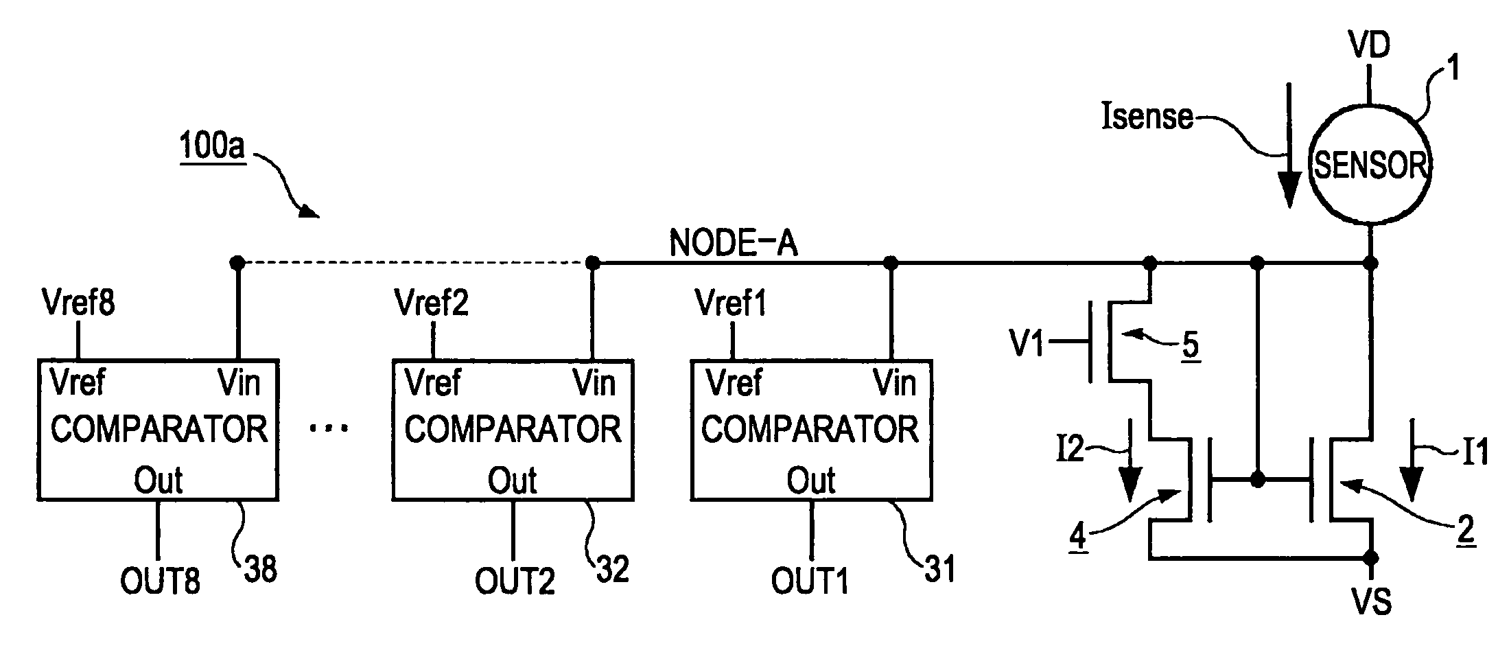
[0071]FIG. 1 is a diagram showing a sensor 1 and an A / D conversion circuit 100a (electronic circuit) realizing an electronic circuit in accordance with a first embodiment of the present invention. Elements that are the same as those of the known structure shown in FIG. 11 are designated by the same reference numerals, and a description thereof is omitted. Referring to FIG. 1, a transistor 2 (first transistor), a transistor 4 (second transistor), a transistor 5 (control circuit), and transistors constituting comparator circuits 31 to 38 are field-effect transistors each including an active layer made of thin-film polysilicon disposed on a glass substrate (substrate).

[0072]The transistor 2, the transistor 4, and the transistor 5 constitute a current-voltage conversion circuit that converts a current into a voltage. The transistor 4 and the transistor 5 constitute a range-switching circuit that switches the current-voltage conversion range (measurement range) of the current-voltage con...

second embodiment

[0094]FIG. 9 is a circuit diagram showing a sensor 1 and an A / D conversion circuit 100b according to a second embodiment of the invention. Referring to FIG. 9, a transistor 2, a transistor 4, a transistor 15, and a transistor 16 constitute a current-voltage conversion circuit that converts a current into a voltage. The transistor 4, the transistor 15, and the transistor 16 constitute a range-switching circuit that switches the current-voltage conversion range of the current-voltage conversion circuit.

[0095]The transistor 4 is disposed in parallel to the transistor 2, a drain electrode being connected to a Node-A, a source electrode being connected to a power supply voltage VS. A gate electrode of the transistor 4 is connected via the transistor 15 to the Node-A, and connected via the transistor 16 to the power supply voltage VS. A range-switching signal V1 is input into a gate electrode of the transistor 15, and a signal XV1 is input into a gate electrode of the transistor 16.

[0096]...

third embodiment

[0103]FIG. 10 is a circuit diagram showing a sensor 1 and an A / D conversion circuit 100c according to a third embodiment of the invention. Referring to FIG. 10, a transistor 2, a transistor 4, a transistor 8, a transistor 5, and a transistor 7 constitute a current-voltage conversion circuit that converts a current into a voltage. The transistor 4, the transistor 8, the transistor 5, and the transistor 7 constitute a range-switching circuit that switches the current-voltage conversion range of the current-voltage conversion circuit.

[0104]A gate electrode of each of the transistors 2, 4, and 8 is connected to a Node-A, and a source electrode of each of the transistors 2, 4, and 8 is connected to a power supply voltage VS. A drain electrode of the transistor 4 is connected via the transistor 5 to the Node-A, and a drain electrode of the transistor 8 is connected via the transistor 7 to the Node-A. A first range-switching signal V1 is input to the gate electrode of the transistor 5, and...


PUM

PropertyMeasurementUnit
lengthaaaaaaaaaa
widthaaaaaaaaaa
thicknessaaaaaaaaaa

Abstract

An electronic circuit, which has transistors disposed on a substrate, each transistor including an active layer made of thin-film polysilicon, includes a sensor that converts a measured quantity into a current value, a current-voltage conversion circuit that converts the current value into a voltage, and a voltage detection circuit that detects the voltage converted by the current-voltage conversion circuit and outputs a predetermined signal. The current-voltage conversion circuit includes a range-switching circuit that switches a current-voltage conversion range.

Description

BACKGROUND[0001]1. Technical Field[0002]The present invention relates to electronic circuits, electro-optical devices, and electronic apparatuses including the same. More particularly, the invention relates to a circuit formed on a substrate using a thin-film polysilicon deposition technique, a liquid crystal display device including the circuit, and an electronic apparatus including the liquid crystal display device.[0003]2. Related Art[0004]In recent years, a technology in which various thin-film transistor circuits are formed on glass substrates using a low-temperature polysilicon deposition technique, i.e., a System On Glass (SOG) technology, has been actively developed. Examples include a monolithic driver in which a driver circuit is integrated onto a glass substrate of a liquid crystal display.[0005]As one application of the SOG technology, it is conceivable to form a sensor and its sensing circuit on a glass substrate. For example, by using a structure in which an optical se...

Claims


Application Information

Patent Timeline
Patent Type & Authority Patents(United States)
IPC IPC(8): G09G3/38G02F1/133G09G3/20G09G3/36H01L21/822H01L27/04H01L27/146H03M1/18
CPCG09G3/3406G09G3/3648H03M1/361G09G2310/0248G09G2360/144G09G2300/0417H03M1/12G09G3/36G02F1/136
Inventor KOBASHI, YUTAKA
Owner JAPAN DISPLAY WEST
Why Eureka
Try Eureka