Overvoltage-protected light-emitting semiconductor device, and method of fabrication

a technology of overvoltage protection and semiconductor devices, applied in semiconductor devices, semiconductor/solid-state device details, electrical apparatus, etc., can solve the problems of inability to meet the requirements of electrostatic breakdown, inability to resist electrostatic breakdown, and unsatisfactory solutions, etc., to achieve convenient and economical manufacture, improve the effect of reverse voltage, and reduce the size of the devi

Inactive Publication Date: 2011-03-01
SANKEN ELECTRIC CO LTD
View PDF1 Cites 7 Cited by
  • Summary
  • Abstract
  • Description
  • Claims
  • Application Information

AI Technical Summary

Benefits of technology

[0007]Another object of the invention is to make possible the manufacture of such an overvoltage-protected LED more easily and economically than heretofore.
[0014]The invention presupposes use of a silicon substrate in combination with a light-generating semiconductor region composed of compound semiconductor layers containing a Group III element or elements. In the course of the epitaxial growth of the light-generating semiconductor region on the substrate, there inevitably occurs a thermal dispersion or a thermal diffusion of the group III element or elements from the light-generating semiconductor region into the substrate. The result, as is well known to the semiconductor specialists, is the creation of a p-type impurity-diffused layer in the substrate. The invention makes use of this by-product of the epitaxial growth of the light-generating semiconductor region for equivalently providing a serial connection of two or three overvoltage protector diodes of either pnp or npn configuration which is itself connected in parallel with the light-generating semiconductor region. The overvoltage-protected LEDs according to the invention are therefore more compact in construction, easier and more economical of manufacture, and capable of withstanding higher reverse voltages than heretofore.

Problems solved by technology

These devices have, however, an inherent weakness in withstanding electrostatic breakdown, being susceptible to destruction when subjected to a voltage surge in excess of 100 volts.
This solution is unsatisfactory in consideration of the greater bulk of the resulting device caused by the addition of the discrete overvoltage protector.
This prior art overvoltage-protected LED does not lend itself to use in applications (e.g., LED matrix) where it is required to withstand a higher reverse voltage.
The two additional dopings required made the fabrication of the overvoltage-protected LED unnecessarily time-consuming and costly.

Method used


Image

  • Overvoltage-protected light-emitting semiconductor device, and method of fabrication
  • Overvoltage-protected light-emitting semiconductor device, and method of fabrication
  • Overvoltage-protected light-emitting semiconductor device, and method of fabrication

Examples


Embodiment Construction

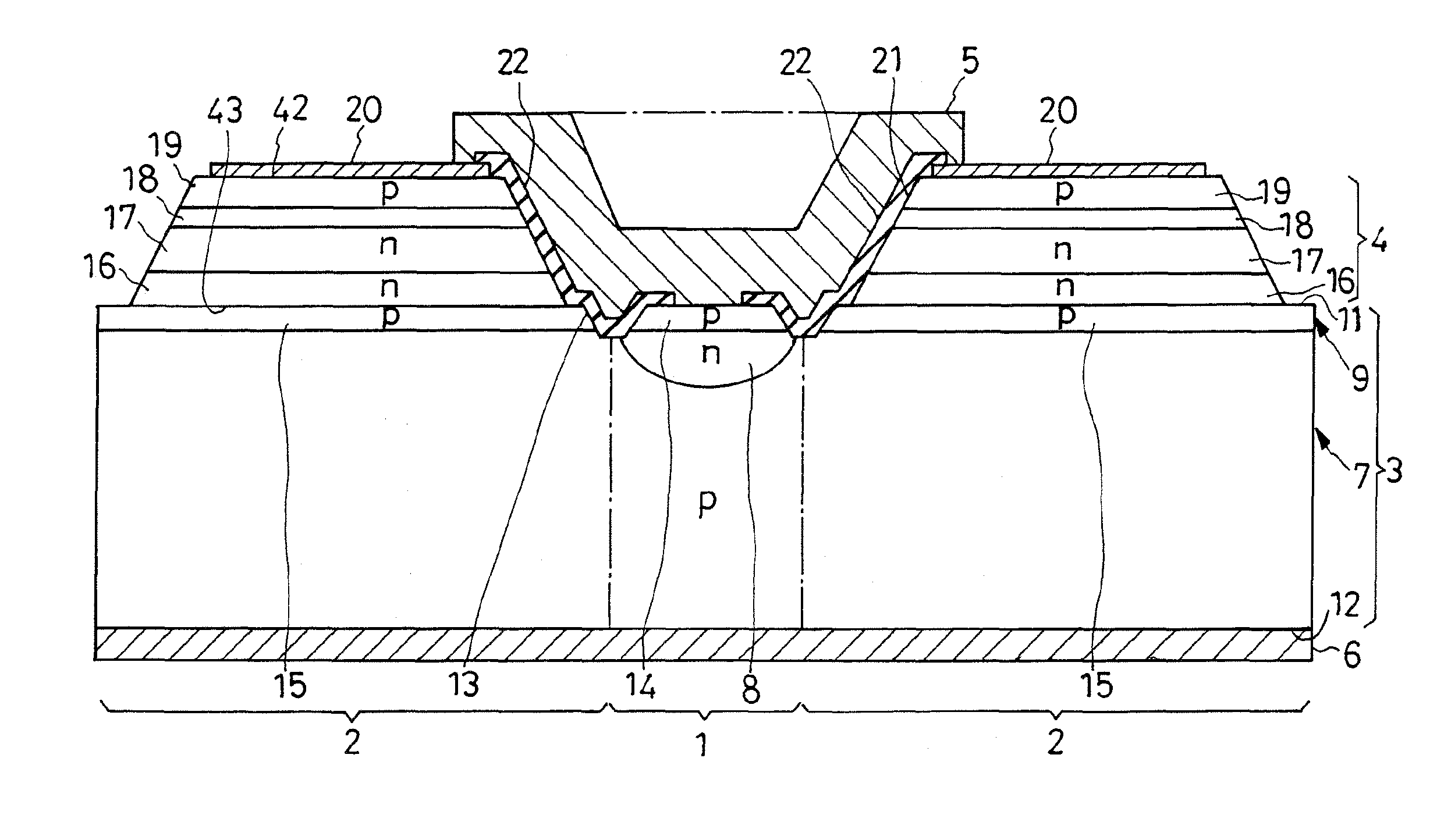
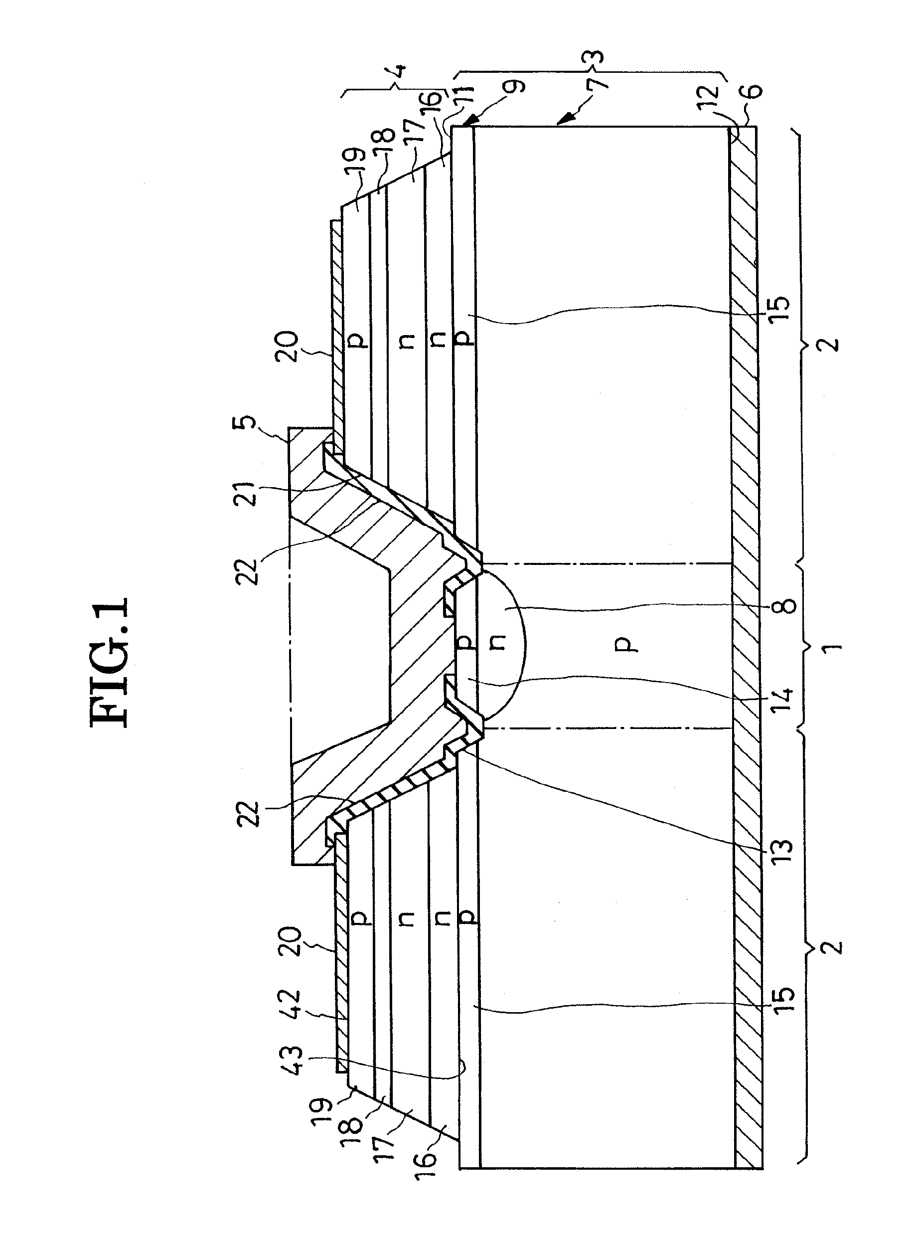
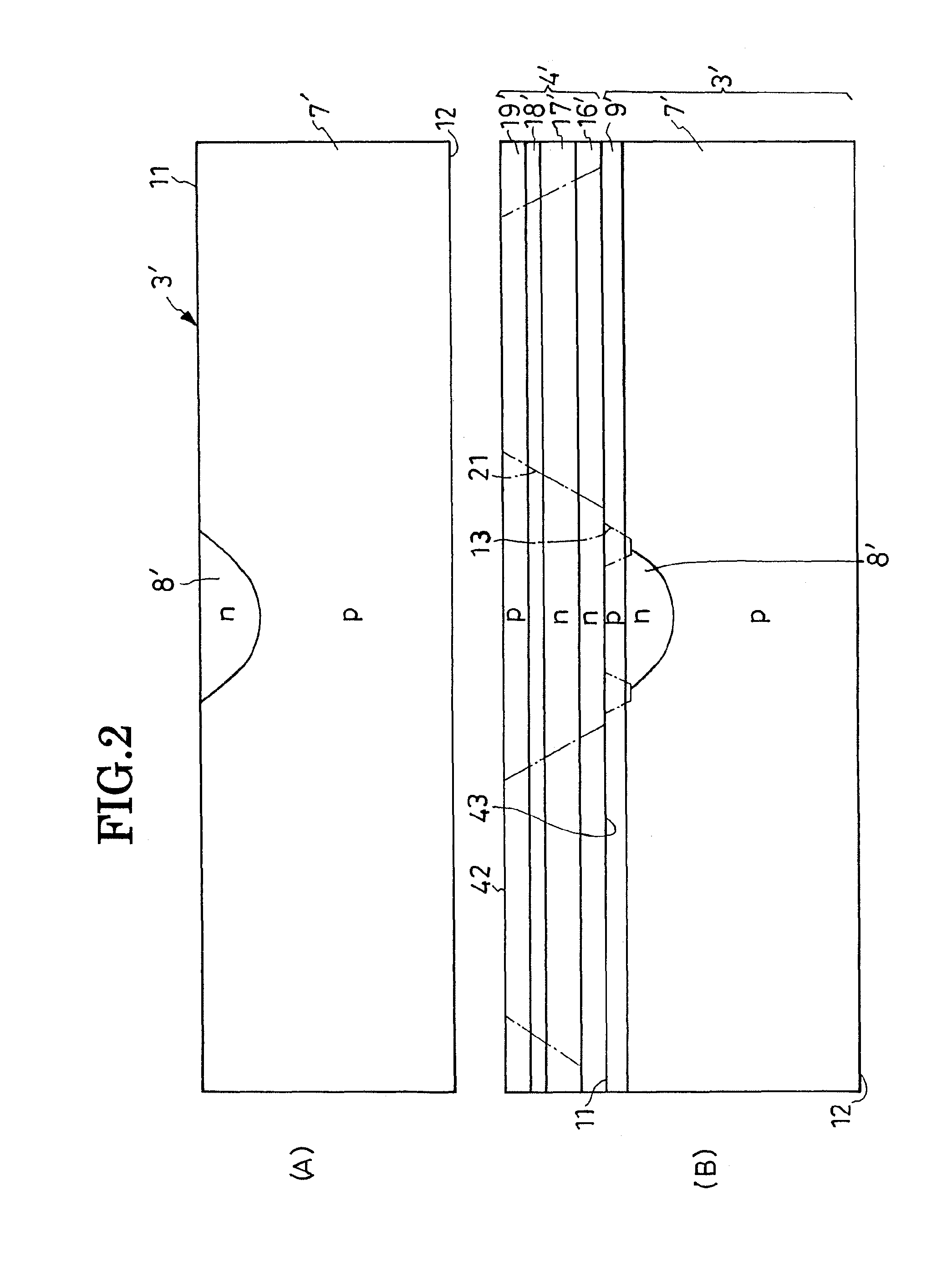
[0032]The present invention is believed to be best embodied in the overvoltage-protected LED illustrated in FIG. 1 of the above drawings. The representative LED includes a silicon substrate 3 which may be notionally divided into an overvoltage protector section 1 and LED section 2. The overvoltage protector section 1, at the central part of the substrate 3, is configured to provide overvoltage protector diodes according to the invention. The LED section 2 surrounds the overvoltage protector section 1 and supports a light-generating semiconductor region 4 thereon. Deposited on the LED section 2, the light-generating semiconductor region 4 is in the form of a lamination of several constituent layers for conventionally generating light. A front or top electrode 5 and back or bottom electrode 6 are disposed opposite each other across the substrate 3 and light-generating semiconductor region 4.

[0033]The substrate 3 is mostly constituted of a region 7 of p-type silicon and additionally ha...


PUM

PropertyMeasurementUnit
wavelength rangeaaaaaaaaaa
voltageaaaaaaaaaa
reverse voltageaaaaaaaaaa

Abstract

A light-generating semiconductor region is grown by epitaxy on a silicon substrate. The light-generating semiconductor region is a lamination of layers of semiconducting nitrides containing a Group III element or elements. The silicon substrate has a p-type impurity-diffused layer formed therein by thermal diffusion of the Group III element or elements from the light-generating semiconductor region as a secondary product of the epitaxial growth of this region on the substrate. The p-type impurity-diffused layer is utilized as a part of overvoltage protector diodes which are serially interconnected with each other and in parallel with the LED section of the device between a pair of electrodes.

Description

CROSS REFERENCE TO RELATED APPLICATIONS[0001]This is a continuation of Application PCT / JP2007 / 050923, filed Jan. 22, 2007, which claims priority to Japanese Patent Application No. 2006-020242 filed Jan. 30, 2006.BACKGROUND OF THE INVENTION[0002]This invention relates to a light-emitting semiconductor device, or light-emitting diode (LED) in common parlance, and more specifically to an LED featuring provisions for protection against overvoltages. The invention also specifically concerns a method of fabricating such an overvoltage-protected LED.[0003]A host of specialists in electroluminescence have focused their attention in recent years on nitride semiconductors as LED materials. LEDs built from these materials emit light in the wavelength range of 365-550 nanometers. These devices have, however, an inherent weakness in withstanding electrostatic breakdown, being susceptible to destruction when subjected to a voltage surge in excess of 100 volts. It might be contemplated to incorpor...

Claims


Application Information

Patent Timeline
Patent Type & Authority Patents(United States)
IPC IPC(8): H01L21/22H01L33/32H01L33/34H01L33/42
CPCH01L27/15H01L23/62H01L33/007H01L2924/0002H01L2924/00
Inventor KAMII, YASUHIRONIWA, AREISATO, JUNJITAZIMA, MIKIO
Owner SANKEN ELECTRIC CO LTD
Why Eureka
Try Eureka