Input termination for delay locked loop feedback with impedance matching

a delay locked loop and input termination technology, applied in the direction of generating/distributing signals, pulse techniques, instruments, etc., can solve the problems of increasing the layout area of the reference output circuit, the resistance of the terminated load module b>102/b> cannot be updated, and the complexity of the output circuit cannot be improved

Active Publication Date: 2011-03-01
INTEGRATED DEVICE TECH INC
View PDF3 Cites 44 Cited by
  • Summary
  • Abstract
  • Description
  • Claims
  • Application Information

AI Technical Summary

Problems solved by technology

However, the resistance of terminated load module 102 cannot be updated during the rising or falling transitions of the feedback clock signal FBCLK, because such updates would interfere with the timing accuracy of reference output circuit 100, and therefore introduce clock jitter.
This timing is accomplished using a quarter-cycle delay circuit, which undesirably adds complexity and increased layout area to reference output circuit 100.

Method used


Image

  • Input termination for delay locked loop feedback with impedance matching
  • Input termination for delay locked loop feedback with impedance matching
  • Input termination for delay locked loop feedback with impedance matching

Examples


Embodiment Construction

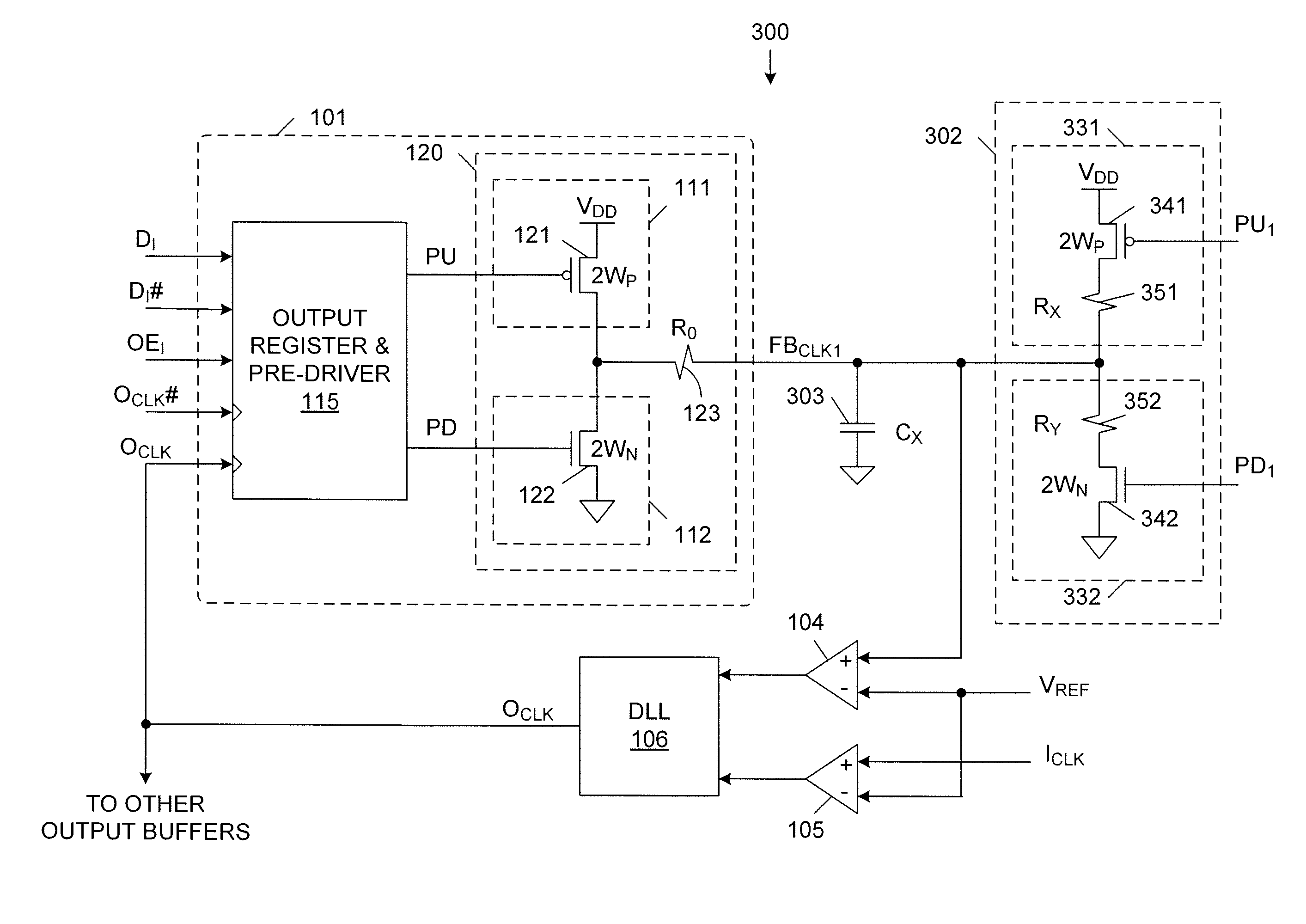
[0039]FIG. 3 is a circuit diagram of a reference output circuit 300 in accordance with one embodiment of the present invention. Because reference output circuit 300 is similar to reference output circuit 100 (FIG. 1), similar elements in FIGS. 1 and 3 are labeled with similar reference numbers. Thus, reference output circuit 300 includes output buffer circuit 101, comparators 104-105 and delay locked loop (DLL) 106. Output buffer circuit 101 includes output register / pre-driver circuit 115 and output driver circuit 120. Output driver circuit 120 includes pull-up circuit 111 (PMOS transistor 121), pull-down circuit 112 (NMOS transistor 122), and resistor 123. As described above in connection with FIG. 1, PMOS pull-up transistor 121 has a channel width of 2WP and an on-resistance of RPM (wherein RPM=KP / 2WP). Similarly, NMOS pull-down transistor 122 has a channel width of 2WN and an on-resistance of RNM (wherein RNM=KN / 2WN). Resistor 123 has a resistance of R0.

[0040]Capacitor 103 of ref...


PUM


Abstract

A reference output circuit for generating an output clock signal for driving signals off of an integrated circuit chip uses a switched terminated load in combination with an output buffer to generate a feedback clock signal, which is used, in combination with a reference input clock signal, to generate the output clock signal. The switched terminated load uses transistors having the same size as transistors in the output buffer. The switched terminated load draws the same DC current as the output buffer. As a result, the switched terminated load and the output buffer have the same electro-migration performance. Pull-up and pull-down MOS impedances of the switched terminated load are easily adjusted during switching periods of the switched terminated load. The design of the switched terminated load minimizes variations in the terminated load impedance due to MOS impedance variations.

Description

FIELD OF THE INVENTION[0001]The present invention relates to an output circuit of an integrated circuit device. More specifically, the present invention relates to a circuit and method for generating an output clock signal in an integrated circuit device.RELATED ART[0002]FIG. 1 is a block diagram of a reference output circuit 100 of a conventional integrated circuit. Reference output circuit 100 includes reference output buffer 101, terminated load module 102, capacitor 103, comparators 104-105 and delay locked loop (DLL) circuit 106. Reference output buffer 101 includes output register / pre-driver circuit 115 and output driver module 120. Output driver module 120, in turn, includes pull-up circuit 111 (i.e., PMOS transistor 121), pull-down circuit 112 (i.e., NMOS transistor 122) and resistor 123. Terminated load module 102 includes pull-up circuit 131 (i.e., PMOS transistor 141 and resistor 151) and pull-down circuit 132 (i.e., NMOS transistor 142 and resistor 152).[0003]Output regi...

Claims


Application Information

Patent Timeline
Patent Type & Authority Patents(United States)
IPC IPC(8): H03K17/16
CPCH03K19/0005H03L7/0812
Inventor WONG, TAK KWONG
Owner INTEGRATED DEVICE TECH INC
Why Eureka
Try Eureka