Display device, electronic device and method of driving display device

a display device and electronic technology, applied in the field of display devices, can solve the problems of difficult to form pixels for each color, and the organic layer is not deposited so well,

Inactive Publication Date: 2011-03-01
SEMICON ENERGY LAB CO LTD
View PDF20 Cites 24 Cited by
  • Summary
  • Abstract
  • Description
  • Claims
  • Application Information

AI Technical Summary

Benefits of technology

[0009]In view of the above problem, it is an object of the present invention to provide a display device in which a display method can be changed as appropriate, with a simple pixel configuration.
[0012]Note that various kinds of transistors can be used in the present invention. Therefore, transistors applicable to the present invention are not limited to a particular type. Thus, the present invention can employ a transistor such as a thin film transistor (TFI) using a non-single crystalline semiconductor film typified by amorphous silicon or polycrystalline silicon. Thus, manufacturing can be done at a low manufacturing temperature, at a low cost, devices can be formed over a large substrate or a transparent substrate, or a transistor can transmit light. A MOS transistor, a junction transistor, a bipolar transistor formed with a semiconductor substrate or an SOL substrate, or the like can also be used. Thus, transistors with less variation, transistors with high current supply ability, or transistors with small size can be formed, or less power consumption circuits can be obtained. In addition, a transistor formed with a compound semiconductor such as ZnO, a-InGaZnO, SiGe or GaAs, a thin film transistor thereof or the like can be applied. Thus, manufacturing can be done at a low manufacturing temperature or at room temperature, or a transistor can be formed directly on a low heat resistant substrate such as a plastic substrate or a film substrate, for example. A transistor obtained by an ink-jet method or a printing method can also be used. Thus, manufacturing at room temperature or at a low vacuum degree, or a manufacturing with use of a large substrate is possible. Since manufacturing without a mask (reticle) is possible, layout of a transistor can be changed easily. A transistor using an organic semiconductor or a carbon nanotube, or other transistors can also be applied. Thus, such a transistor can be formed over a flexible substrate. In the case of using a non-single crystalline semiconductor film, it may contain hydrogen or halogen. In addition, a substrate over which transistors are formed is not limited to a particular type, and various kinds of substrates can be used. Accordingly, transistors can be formed over a single crystalline substrate, an SOI substrate, a glass substrate, a quartz substrate, a plastic substrate, a paper substrate, a cellophane substrate, a stone substrate, a stainless steel substrate, a substrate including a stainless steel foil, or the like. Alternatively, after forming a transistor over a certain substrate, the transistor may be transferred to another substrate. By using such a substrate, a transistor having excellent characteristics or a transistor with low power consumption can be formed, or a nonbreakable device or a heat-resistant device can be manufactured.
[0013]Note also that the structure of a transistor is not limited to a particular type and various structures may be employed. For example, a multi-gate structure having two or more gates may be used. In the case of multi-gate structure, since channel regions are connected in series, a structure in which plural transistors are connected in series is obtained. By using a multi-gate structure, off-current can be reduced as well as the withstand voltage can be increased to improve the reliability of the transistor, and even when the drain-source voltage fluctuates at the time when the transistor operates in the saturation region, flat characteristics can be provided without causing variations of a drain-source current. In addition, such a structure that gate electrodes are formed to sandwich a channel may also be employed. By using such a structure that gate electrodes are formed to sandwich a channel, the area of the channel region can be enlarged to increase the value of current flowing therein, and a depletion layer can be easily formed to improve an S value. A structure in which plural transistors are arranged in parallel is obtained, when gate electrodes are formed to sandwich a channel. In addition, any of the following structures may be employed: a structure where a gate electrode is formed over a channel; a structure where a gate electrode is formed below a channel; a staggered structure; an inversely staggered structure; a structure where a channel region is divided into a plurality of regions, and the channel regions are connected in parallel; or a structure where a channel region is divided into a plurality of regions, and the channel regions are connected in series. In addition, a channel (or a part of it) may overlap a source electrode or a drain electrode. With a structure where a channel (or a part of it) overlaps a source electrode or a drain electrode, unstable operation caused by charges accumulated in a part of the channel can be prevented. In addition, an LDD region may be provided. By providing an LDD region, off-current can be reduced, and the withstand voltage can be increased to improve the reliability of the transistor. Even when the drain-source voltage fluctuates at the time when the transistor operates in the saturation region, stable characteristics can be provided without causing variations in a drain-source current.
[0014]Note that transistors in the present invention may be any type of transistors and may be formed over various types of substrates. Thus, all circuits may be formed over a glass substrate, a plastic substrate, a single crystalline substrate, an SOI substrate, or other substrates. By forming all circuits over one substrate, the number of parts can be reduced to lower manufacturing cost, or connection points with circuit components can be reduced to enhance reliability. Alternatively, such a structure may be employed that a part of circuits is formed over a substrate, while another part of the circuits is formed over another substrate. That is, all circuits are not required to be formed over the same substrate. For example, such a structure may be employed that a part of circuits is formed over a glass substrate with transistors, while another part of the circuits is formed over a single crystalline substrate so that the IC chip is attached onto the glass substrate by COG (Chip on Glass). Alternatively, the IC chip may be connected to the glass substrate by TAB (Tape Automated Bonding) or by using a printed board. In this manner, by forming a part of circuits over the same substrate, the number of parts can be reduced to lower manufacturing cost, or connection points with circuit components can be reduced to enhance reliability. In addition, since a portion of high driving voltage or a portion of a high driving frequency consumes a lot of power, such a portion is not allowed to be formed over the same substrate, and thus, increase in power consumption can be prevented.
[0028]In accordance with the present invention, a unit constituting one pixel can be changed in accordance with an image. As a result, characters can be displayed clearly and imaged can be displayed smoothly.

Problems solved by technology

However, it is difficult to form pixels for each color when the hexagonal pixel configuration is employed.
In particular, in a case of an organic EL element, since an organic layer is deposited for each color, the organic layer is not deposited so well, in the case of such a complex structure.

Method used


Image

  • Display device, electronic device and method of driving display device
  • Display device, electronic device and method of driving display device
  • Display device, electronic device and method of driving display device

Examples


embodiment mode 1

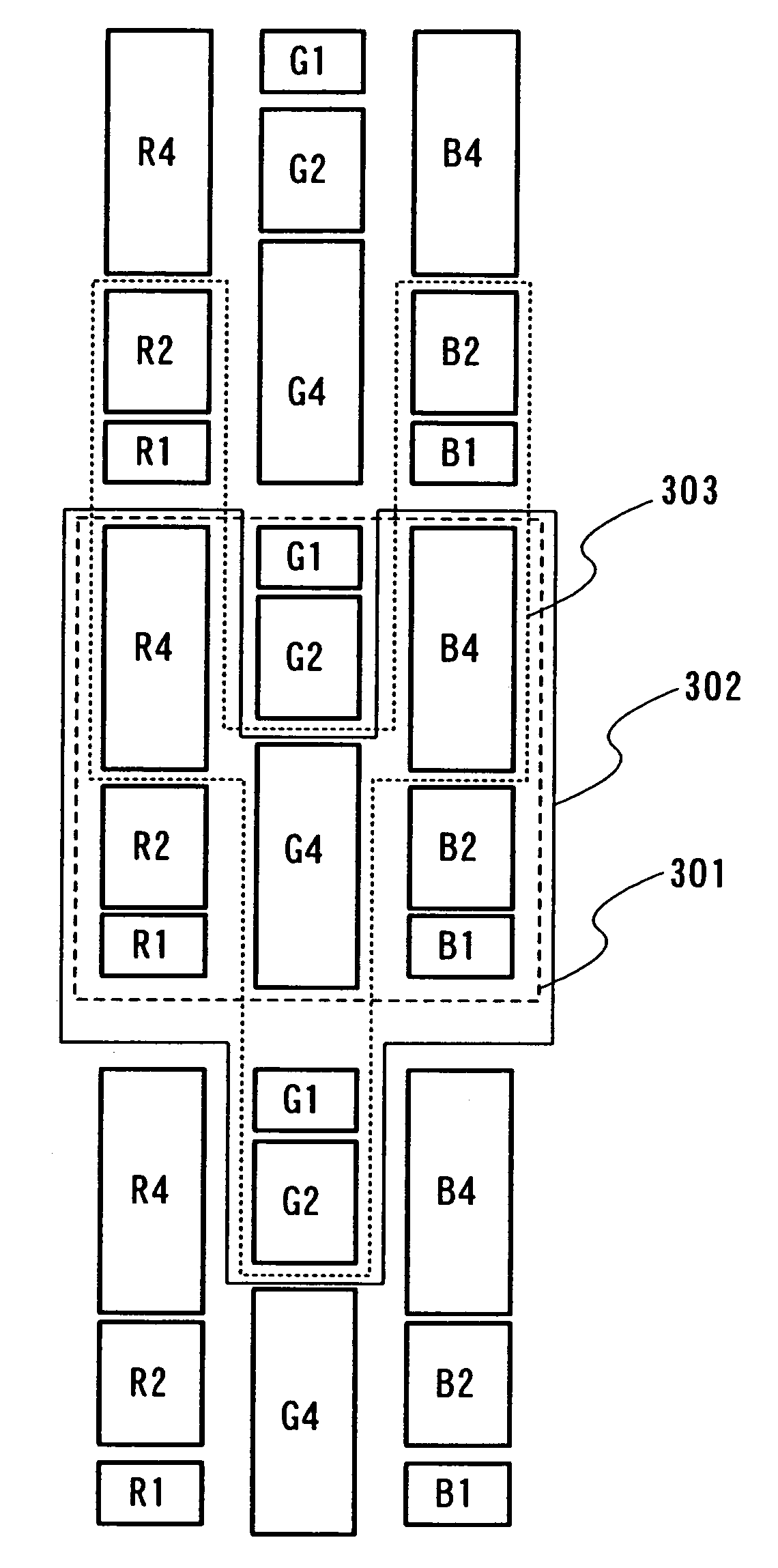
[0080]FIG. 1 shows a pixel configuration of three pixels. Usually, a region 101 corresponds to one pixel.

[0081]R1 and R2 constitute a red sub-pixel, G1 and G2 constitute a green sub-pixel, and B1 and B2 constitute a blue sub-pixel. One pixel is constituted by the sub-pixels of each color. Here, in R1 and R2, areas contributing to light-emission or displaying is set at R1 and R2=1:2. In G1 and G2, areas contributing light-emission or displaying is set at G1 and G2=1:2. In B1 and B2, areas contributing light-emission or displaying is set at B1 and B2=1:2. Gray scales can be expressed by selecting either, both or none of R1 and R2 so as to emit light (or contributes to displaying). In other words, an area gray scale method can be used. In FIG. 1, a square region (dot) surrounded by a heavy line is a display region constituting a part of a sub-pixel. The shape of this display region is not limited to that shown in FIG. 1. R1 is the smallest display region constituting a part of a red su...

embodiment mode 2

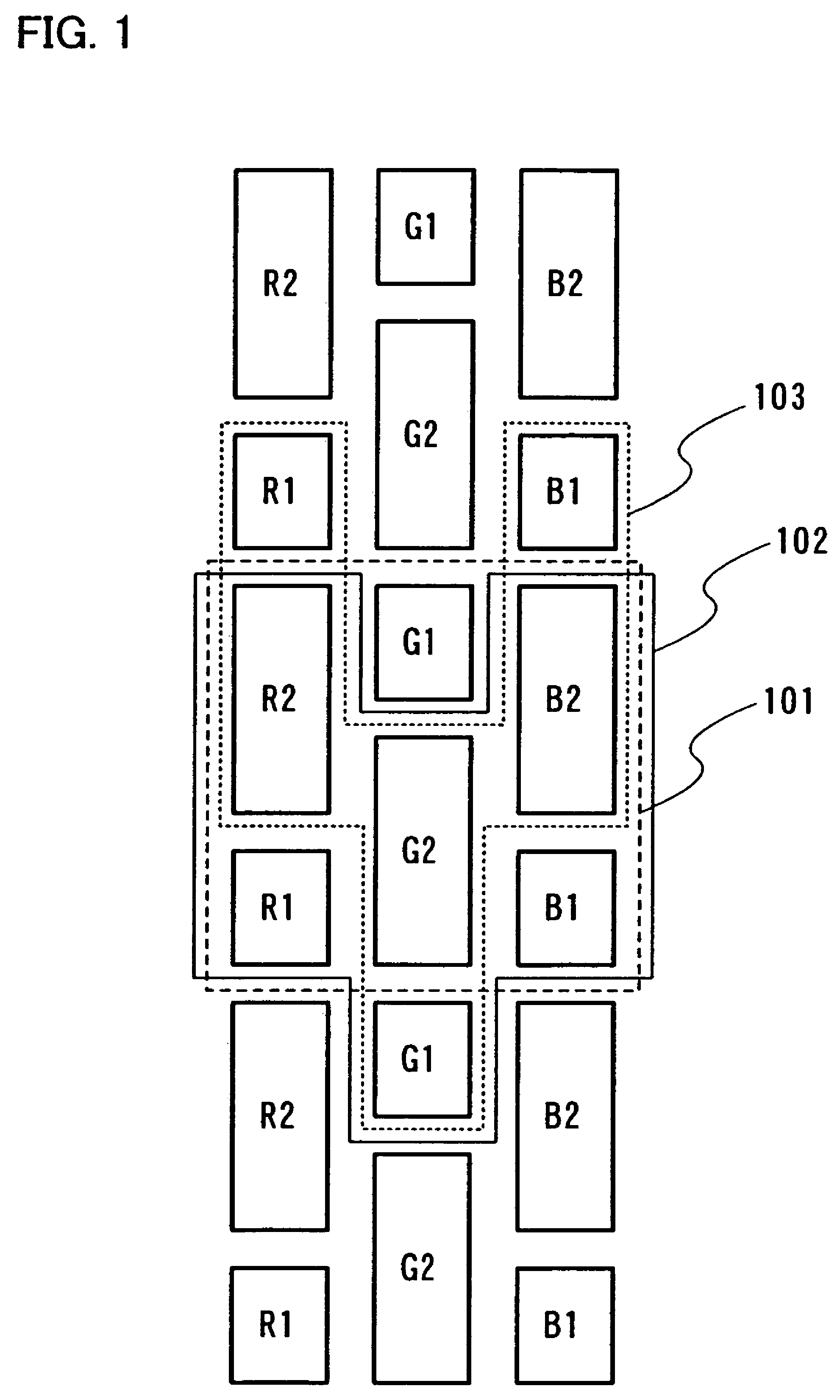
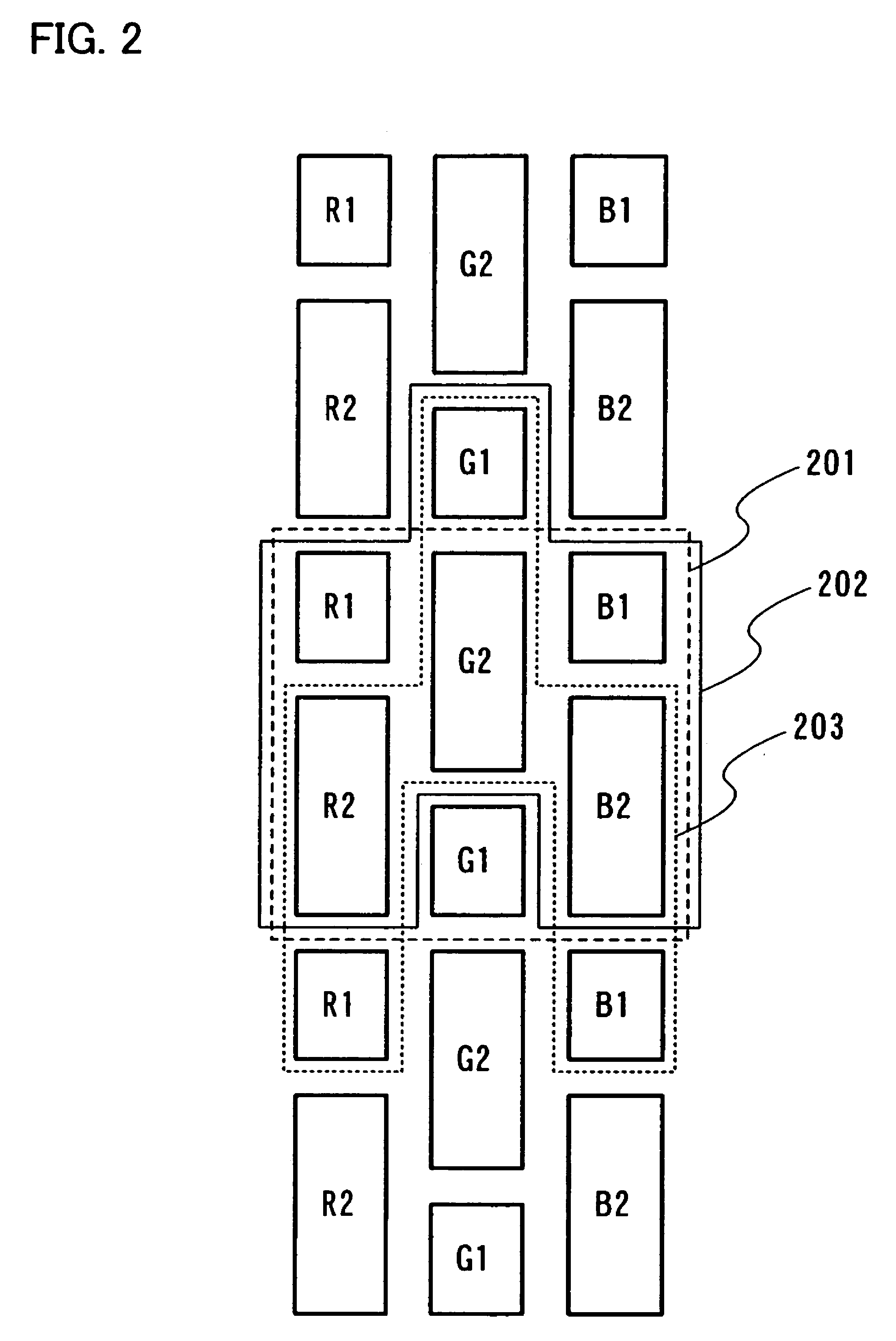
[0096]In Embodiment Mode 2, supply of a signal to each sub-pixel will be described. In FIG. 4, a signal line is arranged for each color and a gate signal line is arranged for each display region of each color. FIG. 4 corresponds to the structure in FIG. 1; however the present invention is not limited to this structure.

[0097]R2 at a second row is connected to a signal line 421 via a selecting transistor 401. R1 at a second row is connected to the signal line 421 via a selecting transistor 402 in other words, R1 and R2 are connected to the same signal line. R2 at a third row is also connected to the signal line 421 via a selecting transistor 403.

[0098]A gate signal line is connected to each selecting transistor. A gate signal line 411 is connected to the selecting transistor 401. A gate signal line 412 is connected to the selecting transistor 402. A gate signal line 413 is connected to the selecting transistor 403. By selecting each gate signal line sequentially, a signal can be suppl...

embodiment mode 3

[0104]Next, an example of a pixel circuit is shown. FIG. 6 shows a pixel of an organic EL. FIG. 6 represents a pixel circuit per one display region.

[0105]A selecting transistor 4904 which is a first transistor is controlled by using a gate signal line 4901 which is a first wire. When the selecting transistor 4904 is turned ON, a video signal is input into a storage capacitor 4905 from a source signal line 4902 which is a second wire. At this time, a driving transistor 4906 which is a second transistor is turned ON / OFF depending on the video signal, and a current flows to an opposite electrode 4908 through a light-emitting element 4907 from a power supply line 4903 which is a third wire.

[0106]Note that the selecting transistor 4904 of FIG. 6 corresponds to the transistors 401 to 403 of FIG. 4, and the transistors 501 to 503 of FIG. 5. In addition, the source signal line 4902 of FIG. 6 corresponds to the signal line 421 of FIG. 4 and the signal line 521 or 522 of FIG. 5.

[0107]Next, FI...


PUM

PropertyMeasurementUnit
depthaaaaaaaaaa
temperatureaaaaaaaaaa
thicknessaaaaaaaaaa

Abstract

The present invention provides a display device which can display characters clearly and display images smoothly. An area gray scale method is adopted and a configuration of one pixel is changed depending on a mode, by selecting one or more display regions in each pixel. When characters are needed to be displayed clearly, one pixel is configured by selecting a stripe arrangement. Thus, clear display can be conducted. When images are needed to be displayed, one pixel is configured by selecting an indented state. Thus, smooth display can be conducted.

Description

BACKGROUND OF THE INVENTION[0001]1. Field of the Invention[0002]The present invention relates to display devices having a display screen on which characters and images are displayed, and relates to a technique for improving visibility of a display screen.[0003]2. Description of the Related Art[0004]In recent years, a so-called self-luminous display device has been attracting attention, which has pixels formed with a light-emitting element such as a light-emitting diode (LED). As a light-emitting element used in such a self-luminous display device, there is an organic light-emitting diode (also called an OLED, an organic EL element, an electroluminescence (EL) element, or the like), which has been attracting attention and used for an EL display (e.g., an organic EL display). Since the light-emitting element such as an OLED is a self-luminous type, it is advantageous, as compared to a liquid crystal display, in that high visibility of pixels is ensured, no backlight is required, high ...

Claims


Application Information

Patent Timeline
Patent Type & Authority Patents(United States)
IPC IPC(8): G02F1/1337G02F1/1335H05B44/00
CPCG09G3/32H01L27/3216G09G3/2085G09G2300/0452G09G2300/08G09G2300/0814H01L27/3244G09G3/3241H10K59/352H10K59/12
Inventor KIMURA, HAJIMEYAMAZAKI, SHUNPEI
Owner SEMICON ENERGY LAB CO LTD
Why Eureka
Try Eureka