Methods of fabricating dual fin structures

a transistor and fin technology, applied in the direction of basic electric elements, electrical equipment, semiconductor devices, etc., can solve the problems of increasing the problem of short channel effects attributable to shortened channel lengths

Active Publication Date: 2011-03-08
MICRON TECH INC
View PDF8 Cites 5 Cited by
  • Summary
  • Abstract
  • Description
  • Claims
  • Application Information

AI Technical Summary

Problems solved by technology

With ever-decreasing semiconductor device feature sizes, the aforementioned short channel effects attributable to shortened channel lengths become increasingly problematic in the fabrication of semiconductor devices.

Method used


Image

  • Methods of fabricating dual fin structures
  • Methods of fabricating dual fin structures
  • Methods of fabricating dual fin structures

Examples


Embodiment Construction

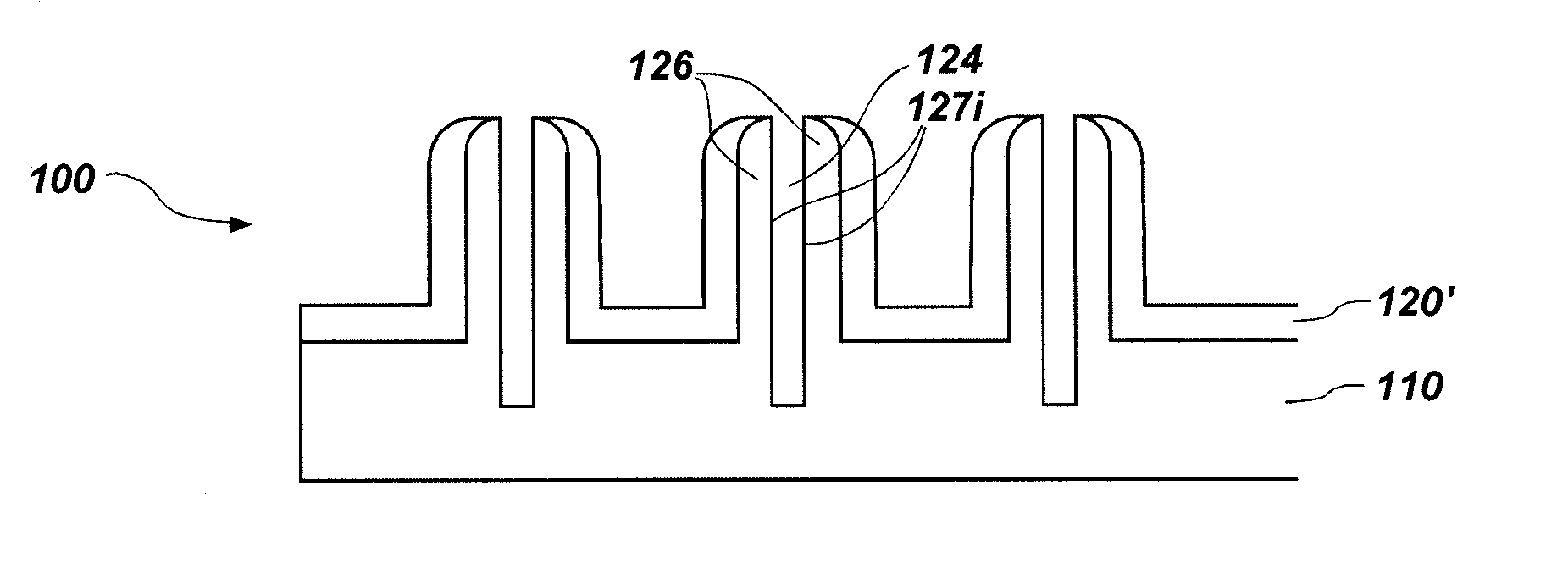
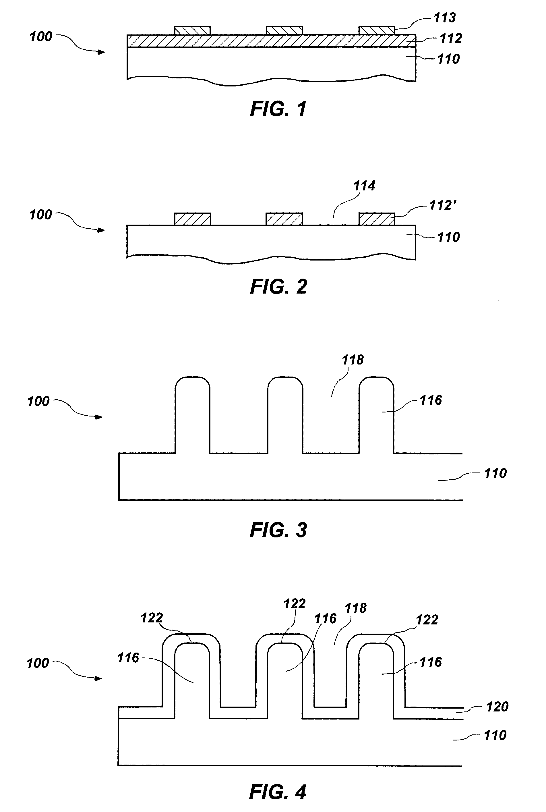
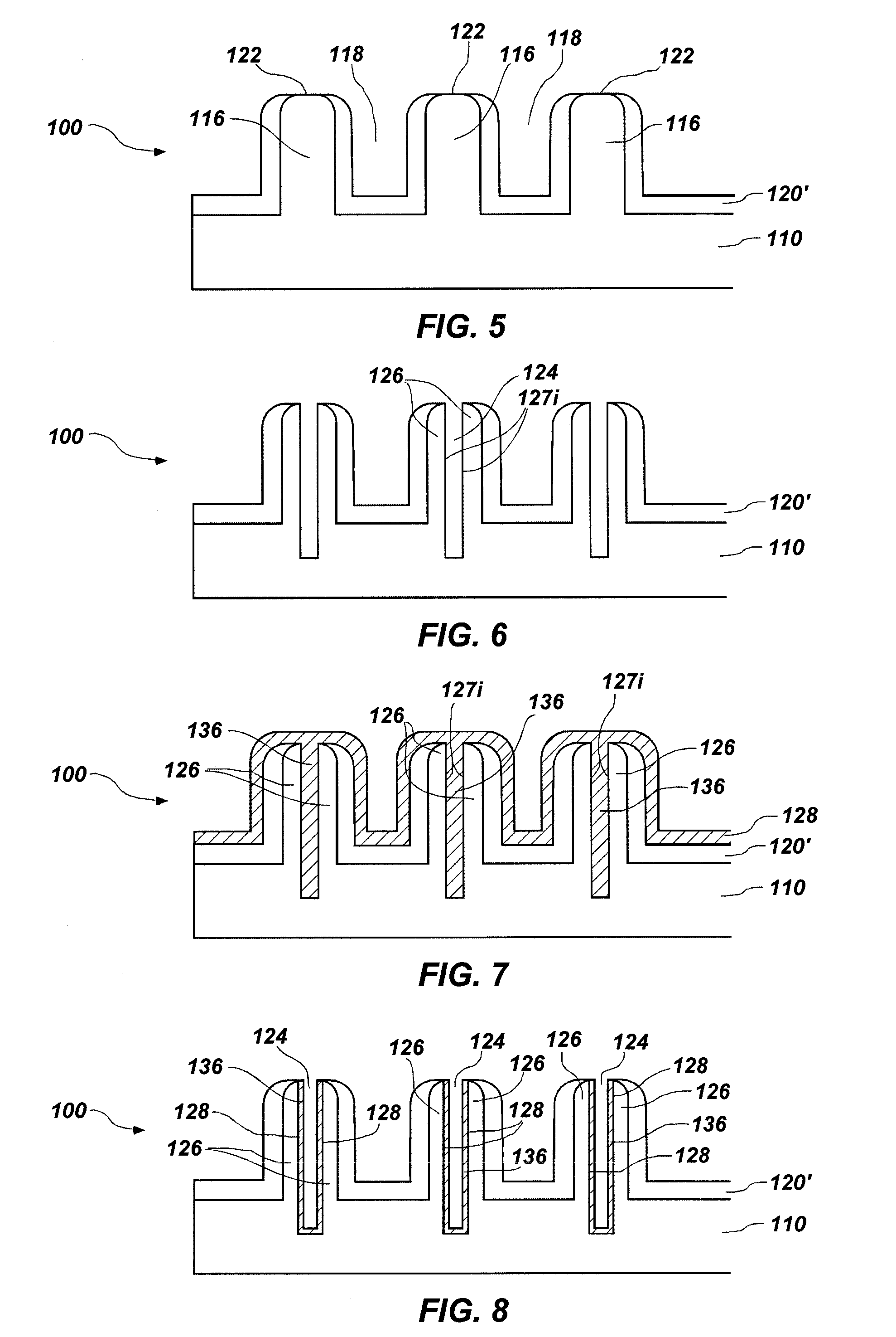
[0009]Embodiments of methods for fabricating semiconductor device structures with dual fins are disclosed, as are embodiments of semiconductor device structures including dual fin-FETs, and systems incorporating same. As used herein, the term “fin” includes a semiconducting material that is etched into a substantially vertically extending structure, relative to a major plane of a substrate on which the structure is formed, that will form the active regions of a semiconductor device such as source, drain and trench. The methods disclosed herein may be used to fabricate a variety of devices such as dynamic random access memory (DRAM) devices, CMOS devices, and other devices in which fin-FETs would be suitable and increases in drive current are desired.

[0010]Reference will now be made to the figures wherein like numerals represent like elements. The figures are not necessarily drawn to scale. Elements in the figures are drawn in cross-section.

[0011]FIGS. 1-6 depict, in simplified cross...


PUM


Abstract

Fin-FET devices and methods of fabrication are disclosed. The Fin-FET devices include dual fins that may be used to provide a trench region between a source region and a drain region. In some embodiments, the dual fins may be formed by forming a trench with fin structures on opposite sides in a protruding region of a substrate. The dual fins may be useful in forming single-gate, double-gate or triple-gate fin-FET devices. Electronic systems including such fin-FET devices are also disclosed.

Description

FIELD OF THE INVENTION[0001]Embodiments of the present invention relate generally to methods for fabricating so-called “fin” field effect transistors, or “fin-FETs,” which protrude from an active surface of a semiconducting substrate and, more specifically, to embodiments of methods for fabricating fin-FETs in which each active-device region includes two fins, as well as to semiconductor device structures with dual fins.BACKGROUND OF THE INVENTION[0002]The performance of silicon-based complementary metal-oxide-semiconductor (CMOS) transistors steadily improves as device dimensions shrink. The decreasing size of metal-oxide-semiconductor field-effect transistor (MOSFET) provides improved integrated-circuit performance speed and cost per function. As channel lengths of MOSFET devices are reduced to increase both the operation speed and the number of components per chip, the source and drain regions extend towards each other, occupying the entire channel area between the source and the...

Claims


Application Information

Patent Timeline
Patent Type & Authority Patents(United States)
IPC IPC(8): H01L21/3205
CPCH01L29/66795H01L29/7854
Inventor MCDANIEL, TERRENCE
Owner MICRON TECH INC
Why Eureka
Try Eureka