
Optimizing PCB power and ground connections for lead free solder processes

a technology of lead free solder and power and ground connection, which is applied in the direction of printed circuit manufacturing, printed circuit components, printed circuit incorporation, etc., can solve the problems of high initial cost, poor joint, and much more layout effort, and achieves improved connection quality, reduced heat sinking effect of layers, and high mechanical and electrical reliability

Active Publication Date: 2011-03-08
ORACLE INT CORP
View PDF3 Cites 5 Cited by
  • Summary
  • Abstract
  • Description
  • Claims
  • Application Information

AI Technical Summary

Benefits of technology

Accordingly, the present embodiments provide apparatuses and methods that provide for enhanced connections between PTHs of multi-layer PCBs and electronic component leads, pins or the like, particularly when the components are attached to the multi-layer PCB using a lead-free solder process. The apparatuses and methods improve the likelihood that the PTHs are completely filled with solder thereby advantageously allowing the PCBs to exhibit high mechanical and electrical reliability. Complete filling of PTHs is achieved by configuring the electrically conductive layers within the multi-layer PCB stack in a manner that reduces the heat sinking effects of the layers. In this regard, the PTHs may not directly contact all of the internal ground or power planes, so the heat sinking or heat transfer effects are reduced. This feature enables molten solder to substantially or completely fill an entire PTH before freezing. Various features and embodiments are described in detail below.

Problems solved by technology

They require much more layout effort and higher initial cost than either wire-wrapped or point-to-point constructed circuits, but are much cheaper and faster for high-volume production.
Too little flux will cause poor joints, while too much flux may cause cosmetic or other problems.
As the thickness of a PCB increases (e.g., above 100 mils, 150 mils, 200 mils, or more) and the combined weight of the copper sheets increases (e.g., above 0.5 oz, 1.0 oz, 1.5 oz, 2.0 oz, or more), it may become more difficult to successfully fill the PTHs during the soldering process.
One cause of the increased difficulty is that the molten solder tends to cool (“freeze”) prematurely before it has traveled from the bottom of the PCB to the top.
The problem of premature freezing of the molten solder can be particularly acute when lead free solder is used in the soldering process.
The multiple layers of copper sheets may conduct heat away from the molten solder (i.e., act as heat sinks), causing the solder to freeze prematurely and causing the PTH to be only partially filled with solder (e.g., 75% filled, 50% filled, or less).
When the PTH is only partially filled with solder, the mechanical and electrical integrity of the solder connection may be significantly reduced or may even be ineffective.

Method used


Image

  • Optimizing PCB power and ground connections for lead free solder processes
  • Optimizing PCB power and ground connections for lead free solder processes
  • Optimizing PCB power and ground connections for lead free solder processes

Examples


Embodiment Construction

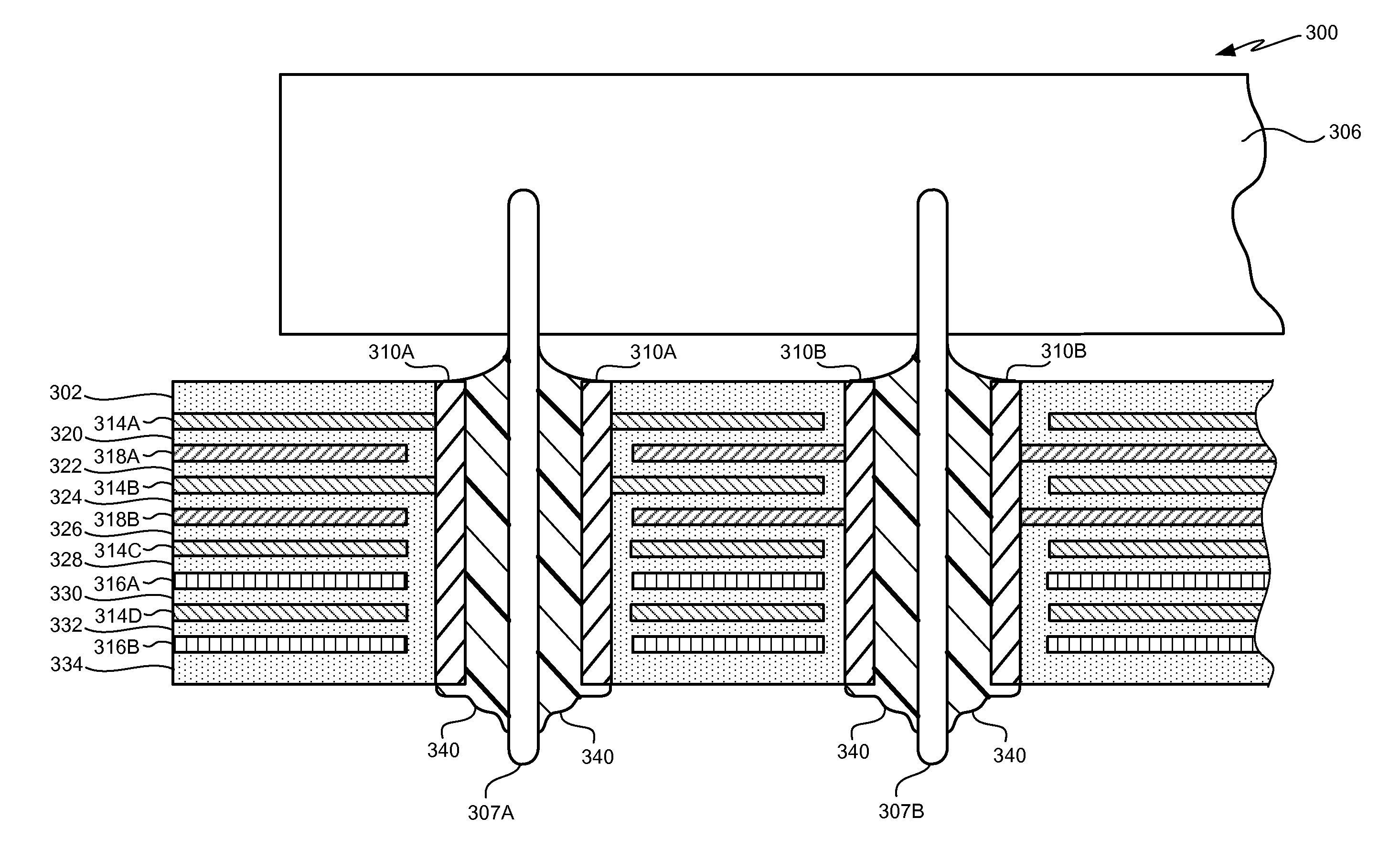
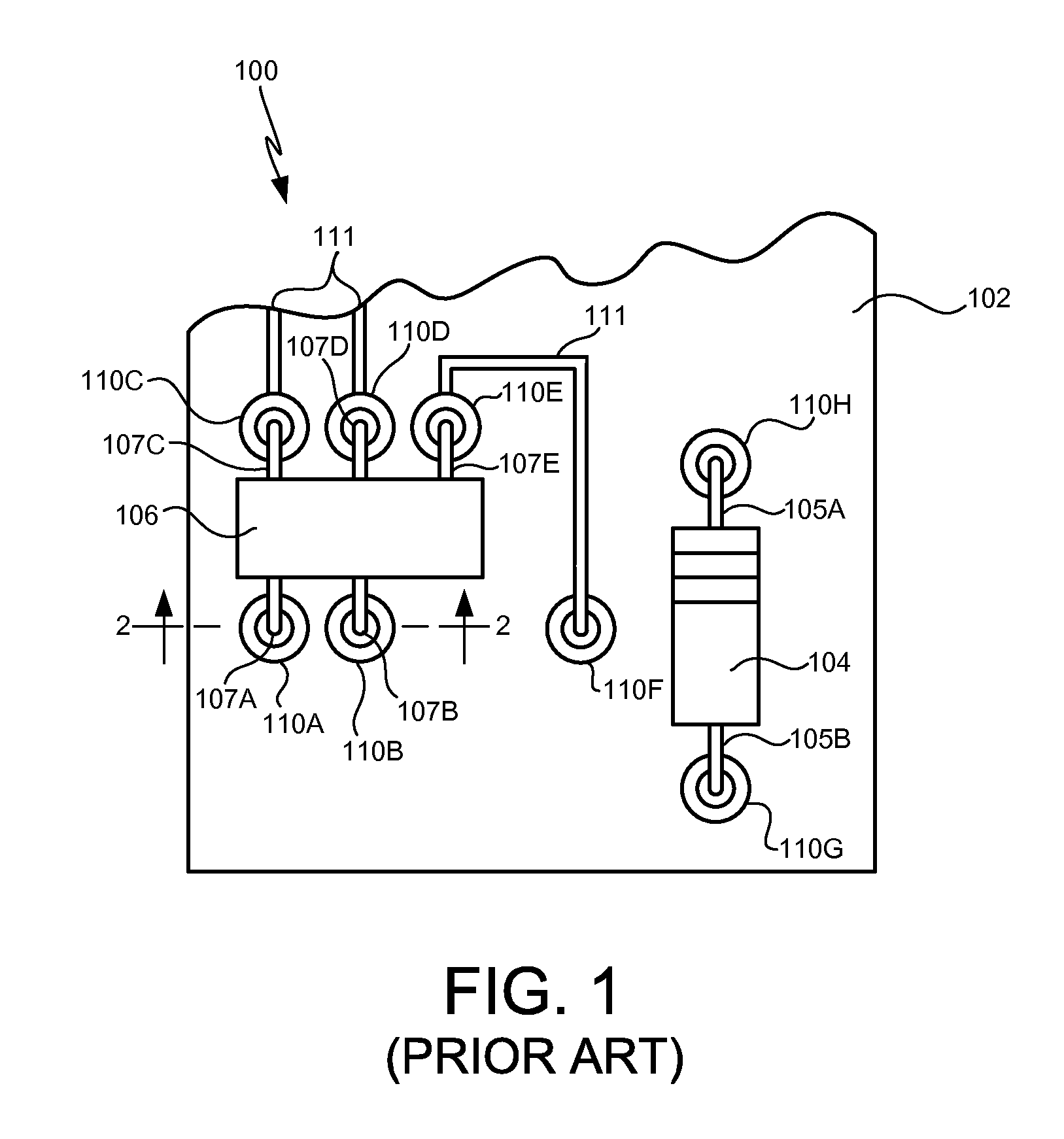
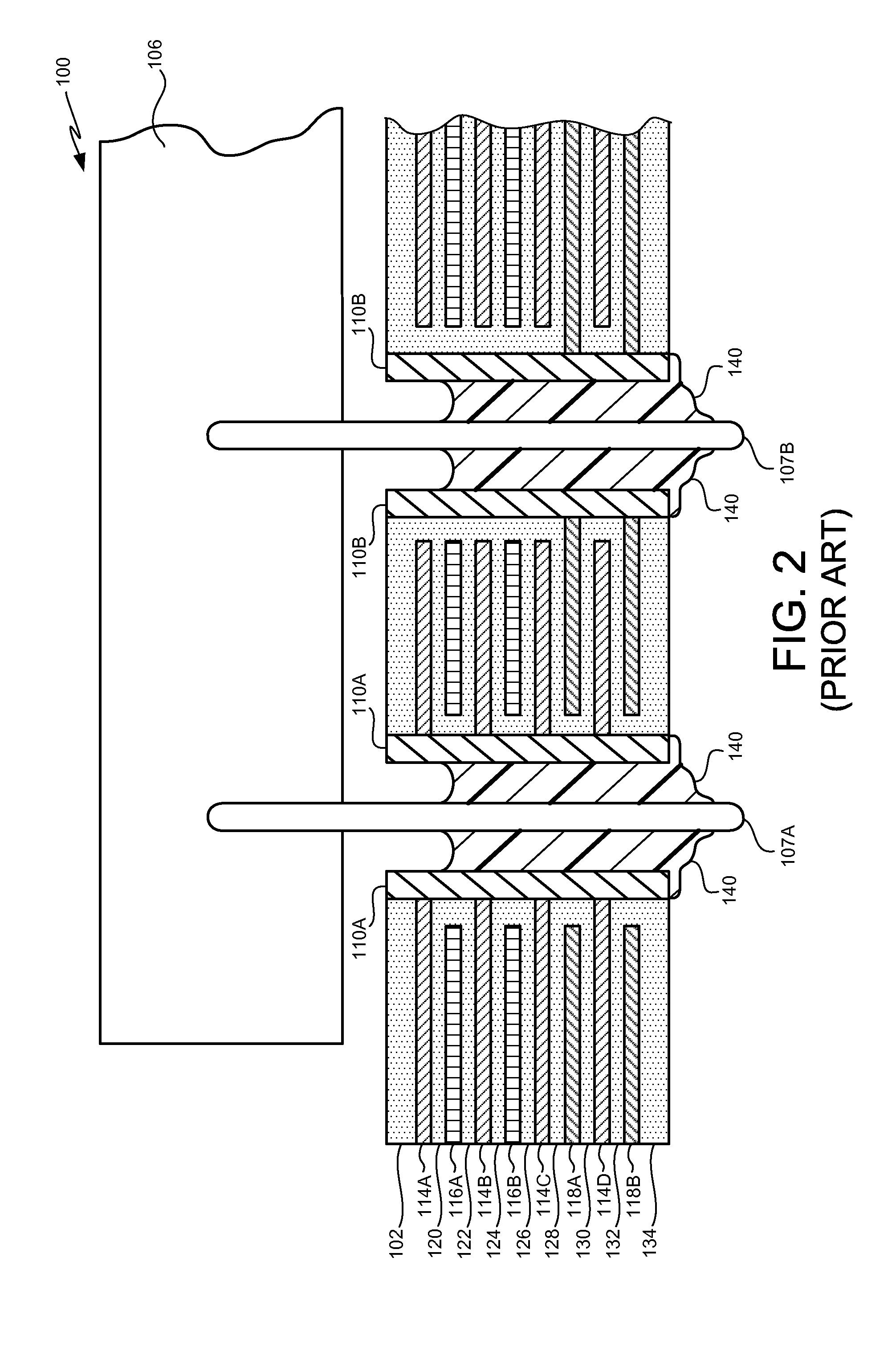
FIGS. 3 and 4 illustrate top and cross-sectional views of a multi-layer PCB 300 that provides enhanced connections with electronic component leads, pins or the like, particularly when the components are attached to the PCB 300 using a lead-free solder process. The top view of FIG. 3 is similar to that of FIG. 1, but as can be seen from the cross-sectional view of FIG. 4, a number of features of the PCB 300 are present that differ from the prior PCB 100 of FIGS. 1 and 2.

The PCB 300 is configured with a resistor 304 and an integrated circuit (IC) 306. The PCB 300 includes a plurality of plated through-holes (PTHs) 310 that may be used to couple electronic components (e.g., the resistor 304 and the IC 306) from the top layer 302 of the PCB 300 to one or more conductors (not shown in FIG. 3) within or on the bottom surface of the PCB 300. In this regard, the PTHs 310 may receive component leads or pins 305A-305B, 307A-307-E extending from the electronic components 304, 306. The PCB 300 ...


PUM

PropertyMeasurementUnit
weightaaaaaaaaaa
weightaaaaaaaaaa
weightaaaaaaaaaa

Abstract

Apparatuses and methods that provide for enhanced connections between PTHs of multi-layer PCBs and electronic component leads, pins or the like, are described herein. The apparatuses and methods improve the likelihood that the PTHs are completely filled with solder thereby advantageously allowing the PCBs to exhibit high mechanical and electrical reliability. Complete filling of PTHs is achieved by configuring the electrically conductive layers within the multi-layer PCB stack in a manner that reduces the heat sinking effects of the layers during the soldering process. In this regard, the PTHs may not directly contact all of the internal ground or power planes, so the heat sinking or heat transfer effects are reduced. This feature enables molten solder to substantially or completely fill an entire PTH before freezing.

Description

BACKGROUND OF THE INVENTIONPrinted circuit boards, or PCBs, are generally used to mechanically support and electrically connect electronic components using conductive pathways, or traces etched from sheets of electrically conductive material (e.g., typically copper sheets) laminated onto a non-conductive substrate. A PCB populated with electronic components is referred to as a printed circuit assembly (PCA), also known as a printed circuit board assembly (PCBA). PCBs are generally rugged, inexpensive, and can be highly reliable. They require much more layout effort and higher initial cost than either wire-wrapped or point-to-point constructed circuits, but are much cheaper and faster for high-volume production. Some PCBs have trace layers inside the PCB and are called multi-layer PCBs, and may, for example, be formed by bonding together separately etched thin boards. Some multi-layer PCBs may include several layers (e.g., 4 layers, 12 layers, 24 layers, or more). Among the layers, t...

Claims


Application Information

Patent Timeline
Patent Type & Authority Patents(United States)
IPC IPC(8): H05K1/11
CPCH05K3/3447H05K3/429H05K3/4641Y10T29/49144H05K2201/062H05K2201/09309H05K2201/0352
Inventor BRITTON, JAMES DAVIDMARTINEZ-VARGAS, JORGE EDUARDO
Owner ORACLE INT CORP
Features
  • Generate Ideas
  • Intellectual Property
  • Life Sciences
  • Materials
  • Tech Scout
  • Unparalleled Data Quality
  • Higher Quality Content
  • 60% Fewer Hallucinations
Learn More