
Photonic memory device, data storing method using the photonic memory device and photonic sensor device

a memory device and sensor technology, applied in the field of memory devices, can solve the problems of inability to realize direct integration of memory devices such as registers or l2 cache memory, inability to manufacture memory devices storing data, and inability to develop memory devices. to achieve the effect of high degree of integration in a small space, high sensitivity and efficient arrangemen

Active Publication Date: 2011-03-08
SEOUL NAT UNIV R&DB FOUND
View PDF5 Cites 6 Cited by
  • Summary
  • Abstract
  • Description
  • Claims
  • Application Information

AI Technical Summary

Benefits of technology

"The present invention relates to a memory device that can be manufactured using photonics technology. The technical effect of this invention is that it provides a more efficient and compact memory device that can be directly integrated onto a photonic circuit, allowing for the storage of data of only 1 bit by combining a plurality of logic circuits. This is in contrast to conventional DRAM or SRAM memory devices that require additional manufacturing processes and have limited integration capabilities. The invention also utilizes the high bandwidth and low latency of photonics technology to provide faster data transmission and higher bandwidth for optical communication networks."

Problems solved by technology

However, a memory device has not been developed yet.
A memory device that is realized by combining photonic logic circuits has a significantly large size, and thus it is very inefficient in respect of integration to manufacture a memory device storing data of only 1 bit by combining a plurality of logic circuits.
That is, when photonics technology is applied substantially, logic circuits or frequency filters can be realized as photonics circuits; however, memory devices such as register or L2 cache memory cannot be realized directly.
For example, a calculation processing unit can realize a logic circuit using a photonic circuit; however, a memory unit cannot directly use a photonic circuit due to the spatial limit and thus has to use conventional DRAM or SRAM.

Method used


Image

  • Photonic memory device, data storing method using the photonic memory device and photonic sensor device
  • Photonic memory device, data storing method using the photonic memory device and photonic sensor device
  • Photonic memory device, data storing method using the photonic memory device and photonic sensor device

Examples


Embodiment Construction

[0024]The present invention will now be described more fully with reference to the accompanying drawings, in which exemplary embodiments of the invention are shown. However, the invention is not limited to the drawings and may be embodied in many different forms.

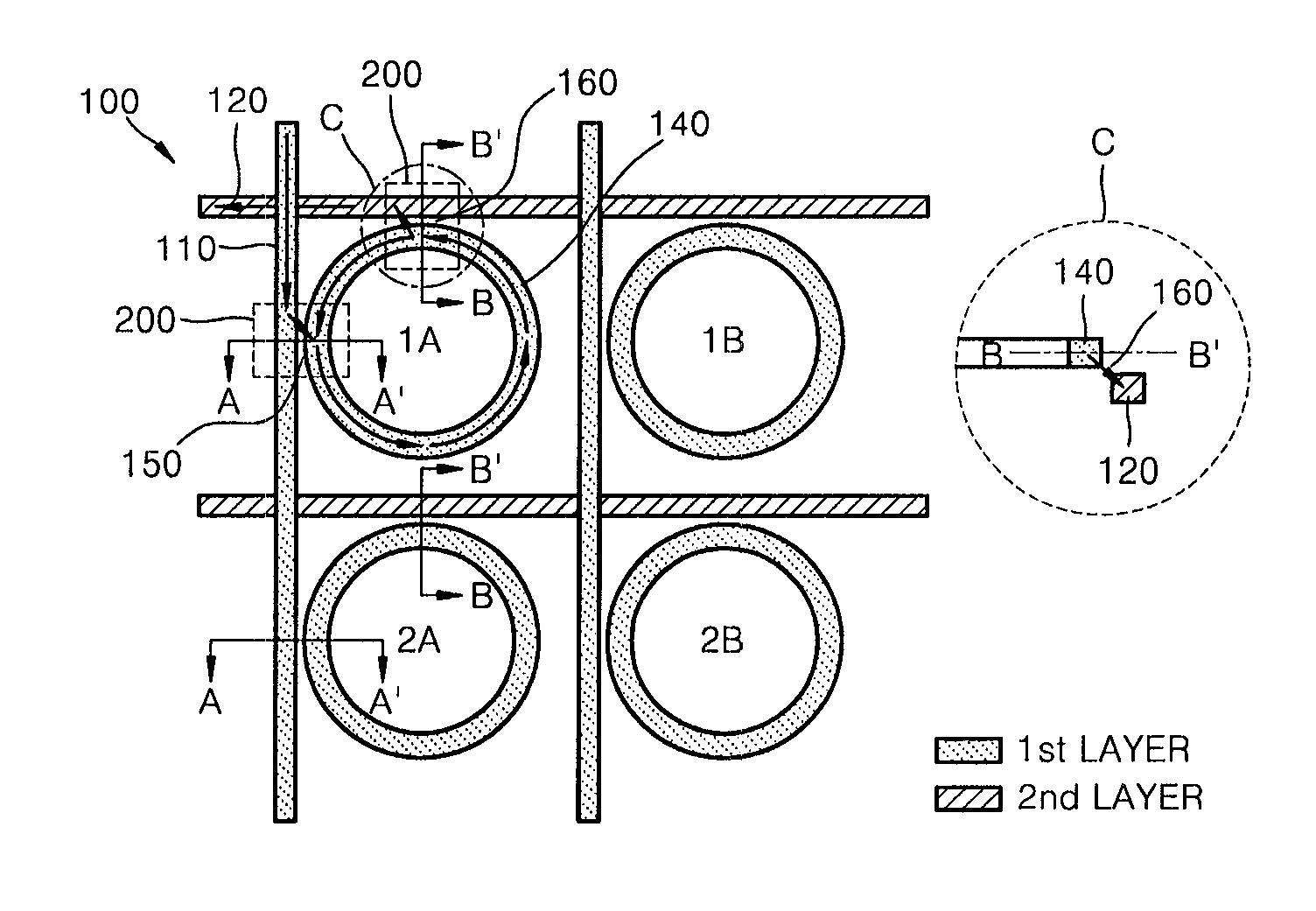
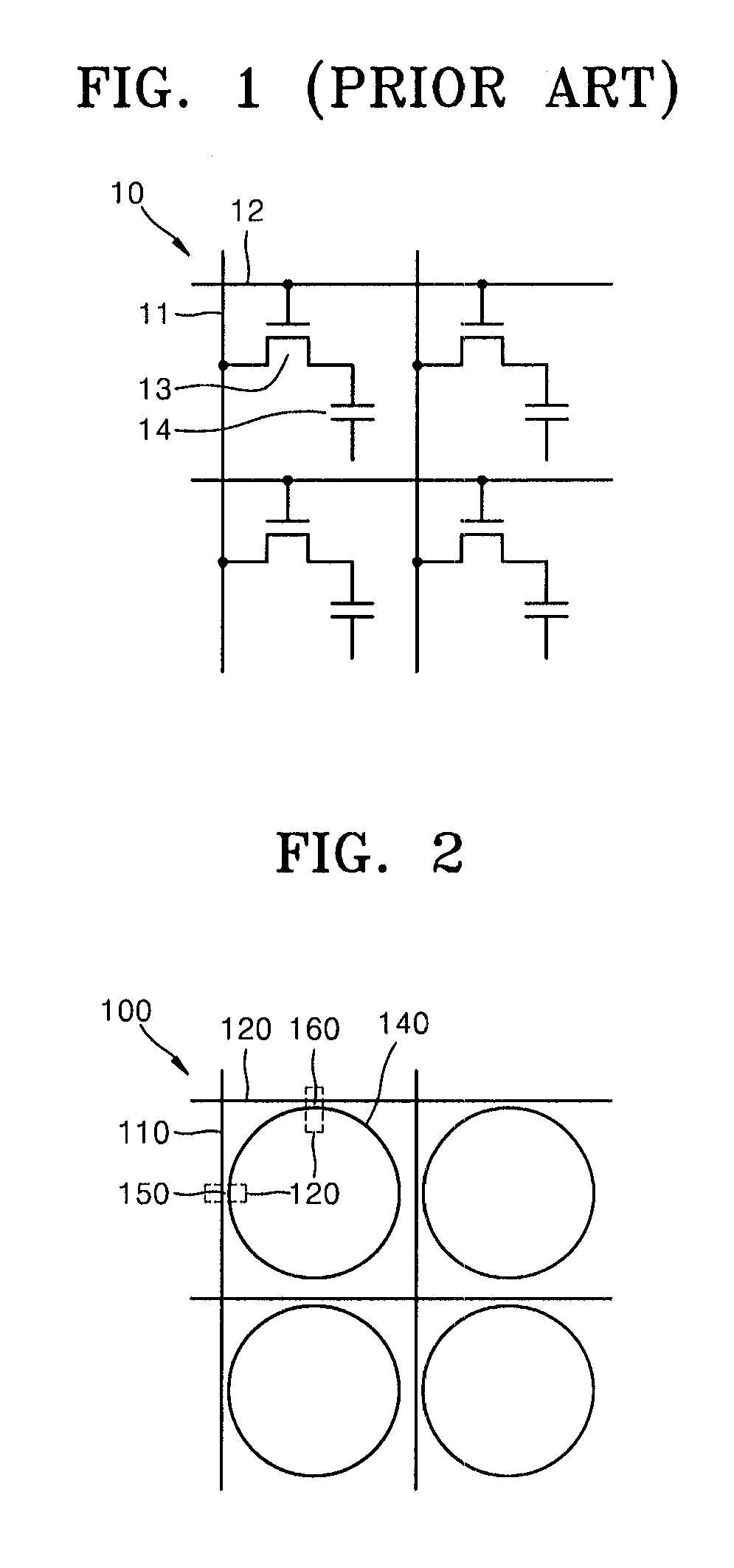
[0025]FIG. 2 is a plane view illustrating a structure of a photonic memory device 100 according to an embodiment of the present invention. Like a DRAM 10 of FIG. 1 using a bit line 11 and a word line 12, the memory device 100 also uses a bit line and a word line. The bit line 11 of FIG. 1 corresponds to a signal line 110 and the word line 12 of FIG. 1 corresponds to a detect line 120 in FIG. 2. The sense amp transistor 13 of FIG. 1 corresponds to a switching device 200 shown in FIG. 5, and the capacitor 14 of FIG. 1 corresponds to a ring resonator 140 in FIG. 2. Electrons are transferred through the bit line 11 and the word line 12 in FIG. 1, while in contrast, photons are transferred through the signal line 110 and the dete...


PUM


Abstract

Provided are a photonic memory device, a method of storing data using the photonic memory device, and a photonic sensor device. The photonic memory device comprises a signal line through which a photon is input; a ring resonator receiving a photon through an input gap that is adjacent to the signal line and storing the photon; and a detect line outputting the photon stored in the ring resonator through an output gap that is adjacent to the ring resonator, wherein data is read / written and stored / deleted by the input / output of the photon.

Description

CROSS-REFERENCE TO RELATED APPLICATIONS[0001]This application is a PCT filing of International Application No. PCT / KR2006 / 005533, filed Dec. 18, 2006, which claims the benefits of earlier filing date and right of priority to Korean Application No. 10-2006-01177077, filed on Nov. 24, 2006, the contents of all of which are incorporated by reference herein their entirety.TECHNICAL FIELD[0002]The present invention relates to a memory device, a method of storing data using the memory device, and a sensor device, and more particularly, to a photonic memory device, a method of storing data using the photonic memory device, and a photonic sensor device capable of detecting external stimulus.BACKGROUND ART[0003]Presently, in computers or information processing devices, data is processed by moving electrons through copper wires; however, recently, photonics technology in which data is transmitted, processed, or computed using a flow of photons is being studied vigorously.[0004]Thanks to the d...

Claims


Application Information

Patent Timeline
Patent Type & Authority Patents(United States)
IPC IPC(8): G11C13/00
CPCG11C11/42G11C13/04G11C7/10
Inventor SONG, BYUNG-YOUNLEE, JUNG-HOON
Owner SEOUL NAT UNIV R&DB FOUND
Learn More