Solid-state imaging device

a solid-state imaging and imaging device technology, applied in the direction of radiation controlled devices, optical radiation measurement, instruments, etc., can solve the problems of reducing the rate of light condensation onto the light-receiving section, increasing the amount of oblique light components being incident on the pixel array section, and reducing the rate of light condensation on the light-receiving section, so as to reduce the sensitivity deterioration, reduce the amount of incident light, and efficiently condense the incident light

Active Publication Date: 2011-03-15
PANASONIC SEMICON SOLUTIONS CO LTD
View PDF10 Cites 10 Cited by
  • Summary
  • Abstract
  • Description
  • Claims
  • Application Information

AI Technical Summary

Benefits of technology

[0011]In view of the above, an object of the present invention is to provide a solid-state imaging device having such a structure that the sensitivity deterioration in the peripheral portion of the imaging area can be suppressed while maintaining the connection between the wiring layers with a simple layout, and a method for producing the same.
[0032]As described above, with a solid-state imaging device and a method for producing the same of the present invention, it is possible to efficiently condense the incident light onto the light-receiving section in the peripheral portion of the imaging area to thereby suppress the sensitivity deterioration, while maintaining the connection between the wiring layers with a simple layout.

Problems solved by technology

Downsizing such a solid-state imaging device will inevitably shorten the inter-pupillary distance of the camera lens, thereby increasing the amount of oblique light component being incident on a pixel array section (an imaging area) in which a plurality of pixels are provided in a two-dimensional arrangement, especially, on a peripheral portion thereof.
Therefore, it is difficult to maintain a high level of image quality.
This reduces the rate of light condensation onto the light-receiving section, thus deteriorating the sensitivity.
Therefore, just shifting the uppermost wiring layer as in the conventional solid-state imaging device is not sufficient for ensuring a desirable sensitivity, with the presence of the lower wiring layers intercepting the incident light to significantly deteriorate the sensitivity.
Where not only the uppermost wiring layer but also the lower wiring layers are to be shifted, it is difficult to realize a solid-state imaging device having such a layout that all elements of wiring layers are shifted because the wiring layers are electrically connected to each other via contacts.

Method used


Image

  • Solid-state imaging device
  • Solid-state imaging device
  • Solid-state imaging device

Examples


first embodiment

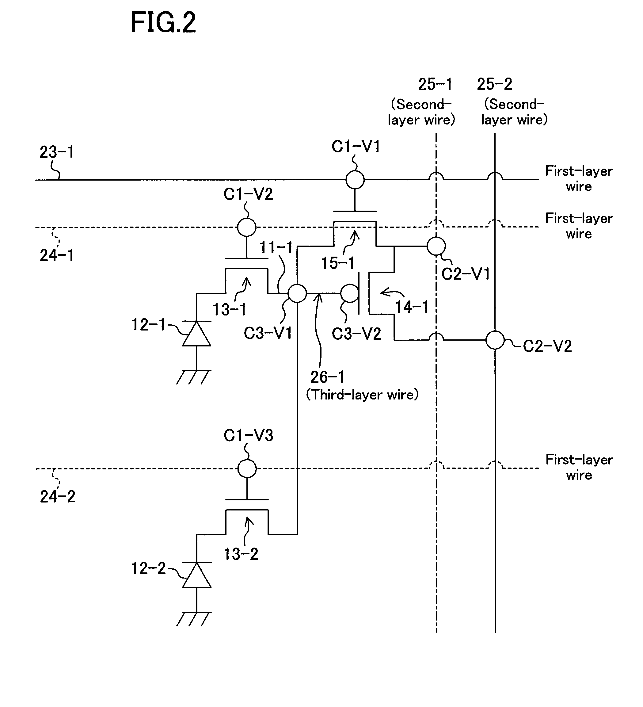
[0048]A solid-state imaging device according to a first embodiment of the present invention will now be described.

[0049]—Basic Configuration of Imaging Area—

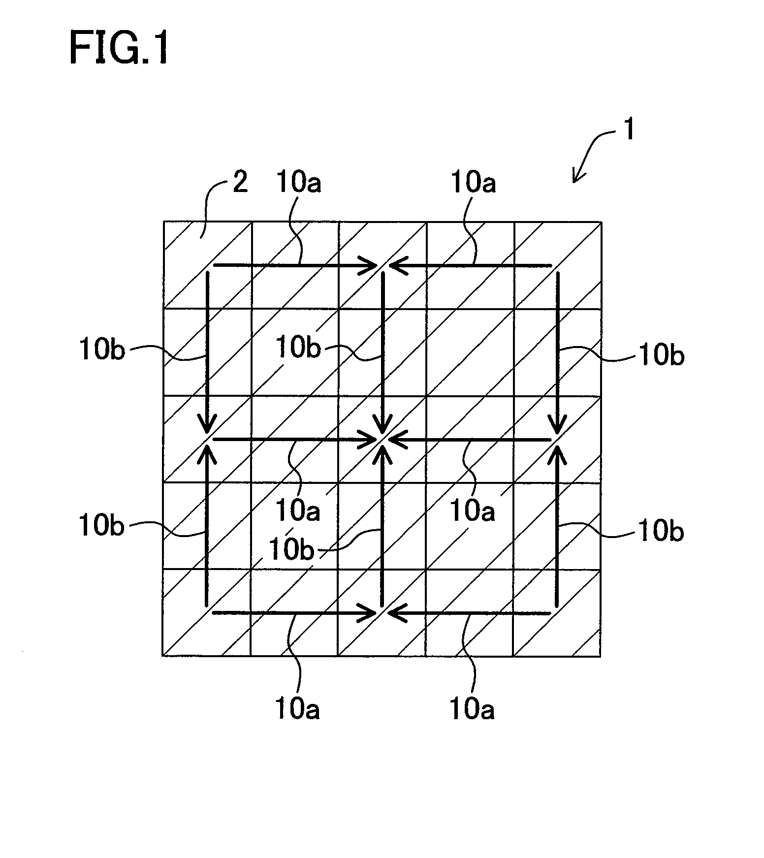
[0050]FIG. 1 is a plan view showing an imaging area of the solid-state imaging device according to the first embodiment of the present invention.

[0051]As shown in FIG. 1, the solid-state imaging device according to the first embodiment of the present invention includes an imaging area (pixel section) 1 where a plurality of unit pixel cells 2 are arranged in a matrix pattern (in the horizontal direction 10a and in the vertical direction 10b) on the semiconductor substrate, the unit pixel cells 2 each including a light-receiving section such as a photodiode for photoelectrically converting the incident light, wherein the charge stored in the light-receiving section is photoelectrically converted to an electric signal, which is detected by a signal detection circuit. The arrows 10a and 10b are shown in FIG. 1 to indicate that “the ...

second embodiment

[0095]A solid-state imaging device according to a second embodiment of the present invention will now be described.

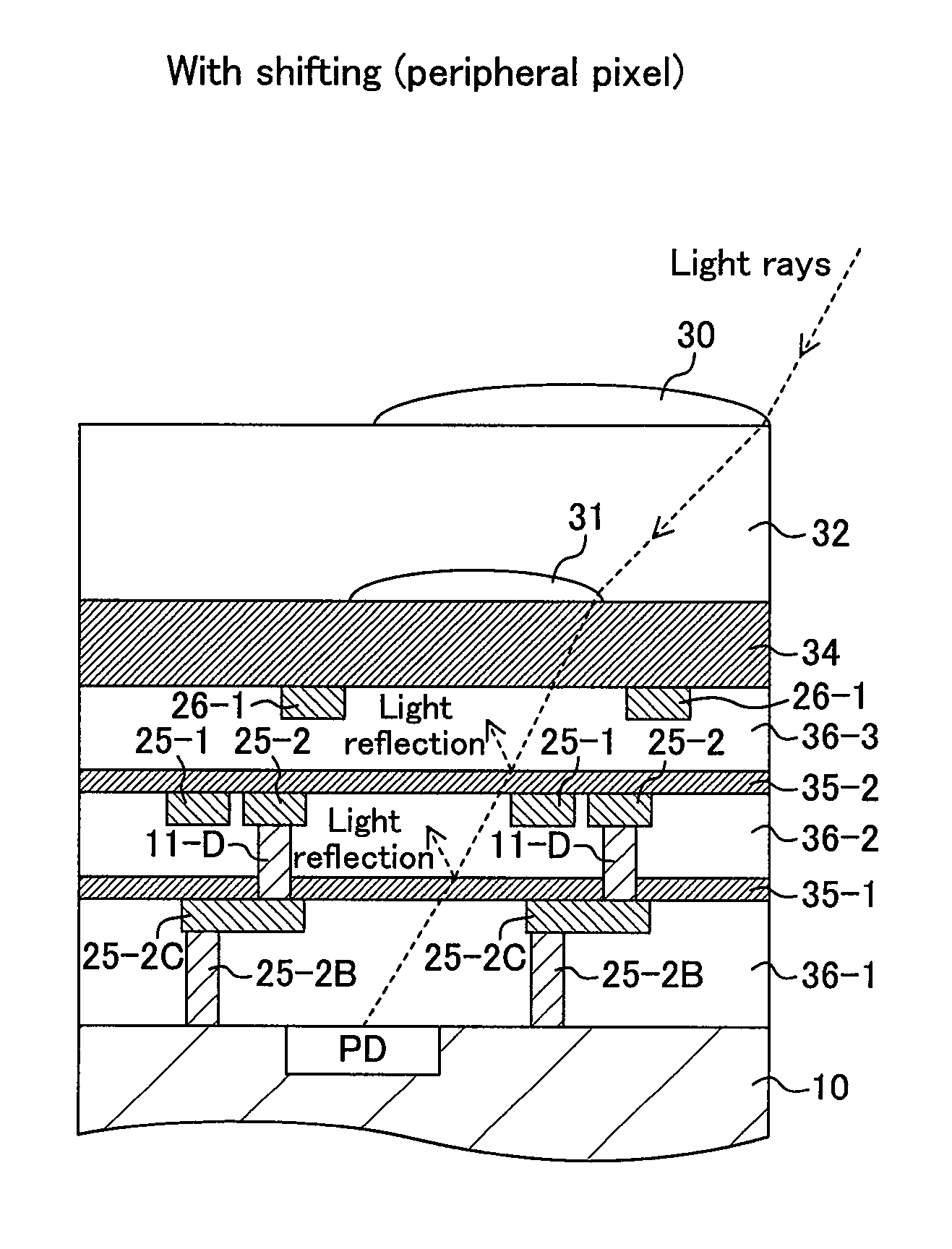
[0096]The solid-state imaging device according to the second embodiment of the present invention has the structure of the solid-state imaging device of the first embodiment described above, i.e., a structure where the arrangement of metal wires and contacts in a peripheral pixel is shifted as described above with respect to that of a corresponding portion in a central pixel, wherein copper wires are used as the metal wires. Therefore, the following description will focus on the characteristic portion of the present embodiment, without repeating the description of what have already been described above in the first embodiment.

[0097]FIG. 10A is a cross-sectional view showing the path of incident light in an arrangement with no wire shifting in a central pixel of a solid-state imaging device according to the second embodiment of the present invention, and FIG. 10B is a cro...


PUM


Abstract

A solid-state imaging device includes a first wiring layer, a second wiring layer, a substrate contact, and a first contact. The arrangement of the substrate contact with respect to a light-receiving section forming a peripheral pixel is shifted, or not shifted, from the arrangement of the substrate contact with respect to a light-receiving section forming a central pixel, by a shift amount r from the peripheral portion toward the central portion. The arrangement of the first contact with respect to the light-receiving section of the peripheral pixel is shifted from the arrangement of the first contact with respect to the light-receiving section of the central pixel, by a shift amount s1 from the peripheral portion toward the central portion. The shift amount s1 is greater than the shift amount r.

Description

BACKGROUND OF THE INVENTION[0001]The present invention relates to a solid-state imaging device including a light-receiving section such as a photoelectric conversion section.[0002]A solid-state imaging device such as a MOS image sensor, for example, typically employs a structure including a semiconductor substrate with light-receiving sections (photoelectric conversion sections such as photodiodes) provided thereon, and various films such as light-blocking patterns and wiring patterns provided in multiple layers on the semiconductor substrate. Downsizing such a solid-state imaging device will inevitably shorten the inter-pupillary distance of the camera lens, thereby increasing the amount of oblique light component being incident on a pixel array section (an imaging area) in which a plurality of pixels are provided in a two-dimensional arrangement, especially, on a peripheral portion thereof. For each pixel, as the angle of incidence of light is greater, light is more blocked by wir...

Claims


Application Information

Patent Timeline
Patent Type & Authority Patents(United States)
IPC IPC(8): H01L27/146H01L27/14H01L31/10H04N5/335H04N5/357H04N5/369H04N5/374
CPCH01L27/14603H01L27/14609H01L27/14623H01L27/14627H01L27/14636H01L27/14643H01L27/14605
Inventor KATSUNO, MOTONARIMIYAGAWA, RYOHEIOHTSUKI, HIROHISA
Owner PANASONIC SEMICON SOLUTIONS CO LTD
Why Eureka
Try Eureka