Thermal management and method for large scale processing of CIS and/or CIGS based thin films overlying glass substrates

a technology of glass substrates and thermal management, applied in the field of photovoltaic techniques, can solve problems such as inadequateness in various situations, and achieve the effect of cost-effectiveness

Inactive Publication Date: 2011-03-22
CM MFG
View PDF14 Cites 91 Cited by
  • Summary
  • Abstract
  • Description
  • Claims
  • Application Information

AI Technical Summary

Benefits of technology

[0008]It is to be appreciated that the present invention provides numerous benefits over conventional techniques. Among other things, the systems and processes of the present invention are compatible with conventional systems, which allow cost effective implementation. In various embodiments, the temperature control method maintains structure integrity of substrates while providing allows various reactions to occur. There are other benefits as well.

Problems solved by technology

In the process of manufacturing CIS and / or CIGS types of thin films, there are various manufacturing challenges, such as maintaining structure integrity of substrate materials, ensuring uniformity and granularity of the thin film material, etc.
While conventional techniques in the past have addressed some of these issues, they are often inadequate in various situations.

Method used


Image

  • Thermal management and method for large scale processing of CIS and/or CIGS based thin films overlying glass substrates
  • Thermal management and method for large scale processing of CIS and/or CIGS based thin films overlying glass substrates
  • Thermal management and method for large scale processing of CIS and/or CIGS based thin films overlying glass substrates

Examples


Embodiment Construction

[0019]The present invention relates generally to photovoltaic techniques. More particularly, the present invention provides a method and structure for a thin film photovoltaic device using a copper indium diselenide species (CIS), copper indium gallium diselenide species (CIGS), and / or others. The invention can be applied to photovoltaic modules, flexible sheets, building or window glass, automotive, and others.

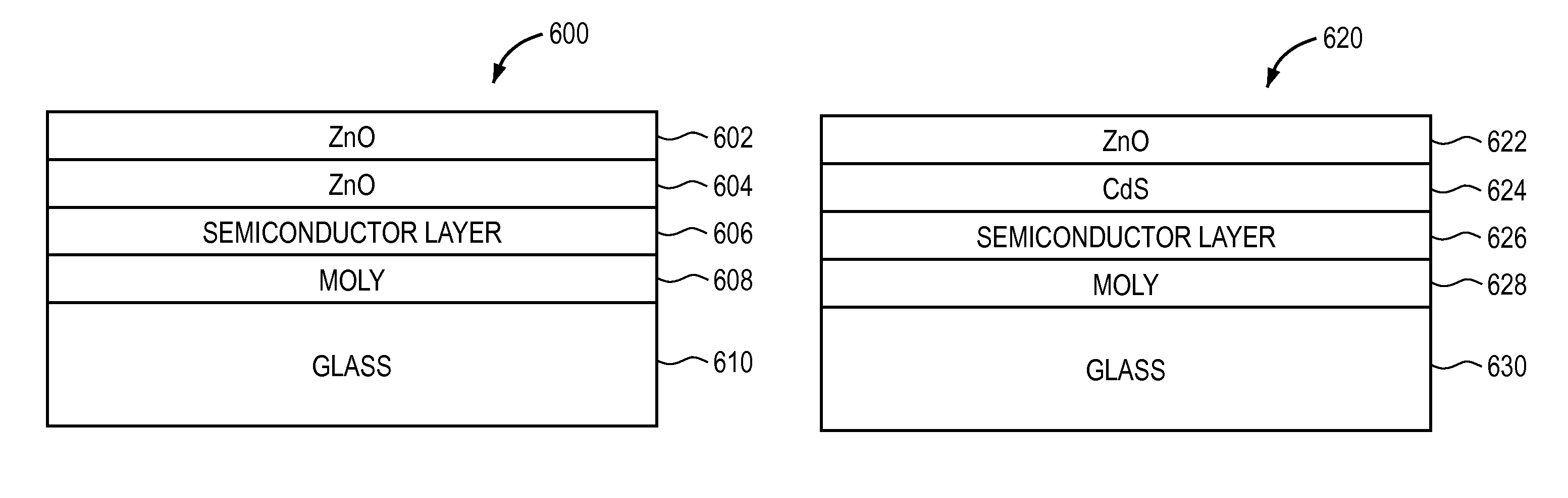
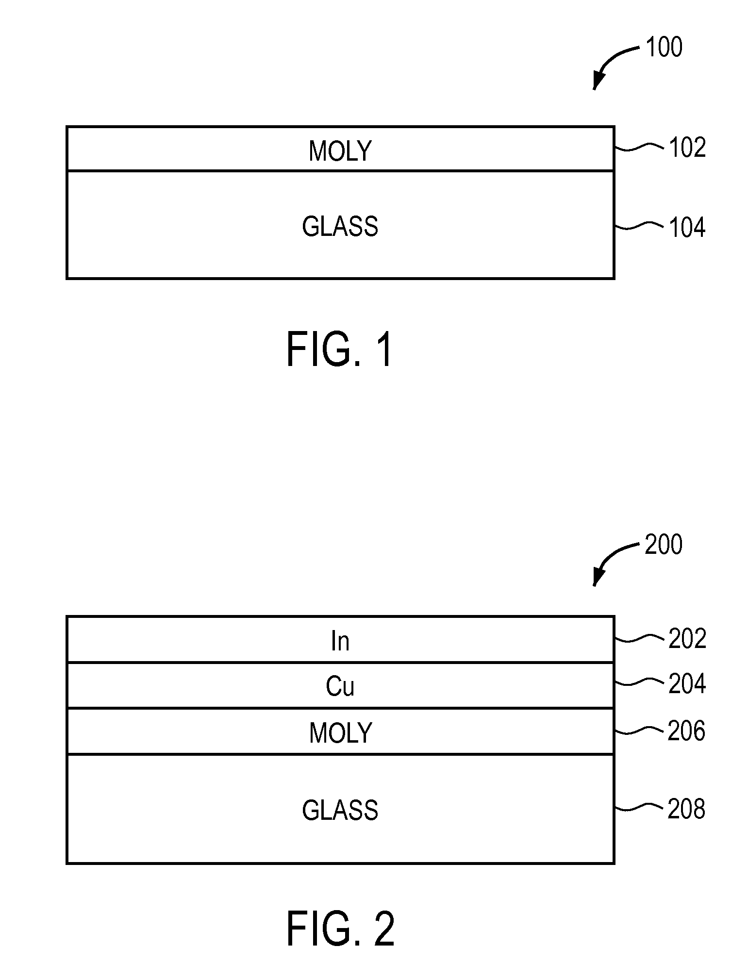
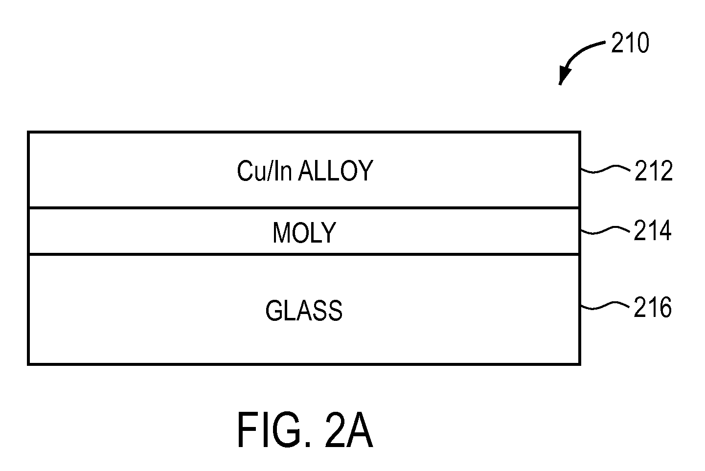
[0020]FIG. 1 is a simplified diagram of a transparent substrate with an overlying electrode layer according to an embodiment of the present invention. This diagram is merely an example, which should not limit the scope of the claims herein. As shown, structure 100 includes a transparent substrate 104. In an embodiment, substrate 104 can be a glass substrate, for example, a soda lime glass. However, other types of substrates can also be used. Examples of substrates include borosilicate glass, acrylic glass, sugar glass, specialty Corning™ glass, and others. As shown, a contact...


PUM

PropertyMeasurementUnit
temperatureaaaaaaaaaa
constant pressureaaaaaaaaaa

Abstract

The thermal management and method for large scale processing of CIS and/or CIGS based thin film overlaying glass substrates. According to an embodiment, the present invention provides a method for fabricating a copper indium diselenide semiconductor film. The method includes providing a plurality of substrates, each of the substrates having a copper and indium composite structure. The method also includes transferring the plurality of substrates into a furnace, each of the plurality of substrates provided in a vertical orientation with respect to a direction of gravity, the plurality of substrates being defined by a number N, where N is greater than 5. The method further includes introducing a gaseous species including a selenide species and a carrier gas into the furnace and transferring thermal energy into the furnace to increase a temperature from a first temperature to a second temperature, the second temperature ranging from about 350° C. to about 450° C. to at least initiate formation of a copper indium diselenide film from the copper and indium composite structure on each of the substrates.

Description

CROSS-REFERENCES TO RELATED APPLICATIONS[0001]This application claims priority to U.S. Provisional Patent Application No. 61 / 101,567, filed Sep. 30, 2008, entitled “THERMAL MANAGEMENT AND METHOD FOR LARGE SCALE PROCESSING OF CIS AND / OR CIGS BASED THIN FILMS OVERLYING GLASS SUBSTRATES” by inventor Robert D. Wieting, commonly assigned and incorporated by reference herein for all purposes.STATEMENT AS TO RIGHTS TO INVENTIONS MADE UNDER FEDERALLY SPONSORED RESEARCH AND DEVELOPMENT[0002]NOT APPLICABLEREFERENCE TO A “SEQUENCE LISTING,” A TABLE, OR A COMPUTER PROGRAM LISTING APPENDIX SUBMITTED ON A COMPACT DISK[0003]NOT APPLICABLEBACKGROUND OF THE INVENTION[0004]The present invention relates generally to photovoltaic techniques. More particularly, the present invention provides a method and structure for a thin film photovoltaic device using a copper indium diselenide species (CIS), copper indium gallium diselenide species (CIGS), and / or others. The invention can be applied to photovoltaic...

Claims


Application Information

Patent Timeline
Patent Type & Authority Patents(United States)
IPC IPC(8): H01L21/00H01L31/00
CPCH01L31/0322H01L31/03923H01L31/1876Y02E10/541Y02P70/50
Inventor WIETING, ROBERT D.
Owner CM MFG
Why Eureka
Try Eureka