Method of forming ONO-type sidewall with reduced bird's beak

a technology of ono-type sidewalls and bird's beaks, which is applied in the direction of semiconductor devices, electrical apparatus, transistors, etc., can solve the problems of small leakage current undesired flow through, material of memory cells, and create problems, so as to reduce the formation of bird's beaks and keep the gate voltage relatively small , good quality

Active Publication Date: 2011-03-22
PROMOS TECH INC
View PDF11 Cites 28 Cited by
  • Summary
  • Abstract
  • Description
  • Claims
  • Application Information

AI Technical Summary

Problems solved by technology

Such sandwiching of different kinds of material layers between the memory cell gates as well as the materials of the memory cell gates can create problems as will be further explained shortly.
A small amount of leakage current can undesirably flow through them.
Contaminating chemicals can pass through pinhole or other defects in the insulators.
However, the inter-gates insulator layer (IGI) that is typically sandwiched between the FG and the CG still poses numerous problems.
The inter-gates insulator layer (IGI) is particularly prone to problems with leakage current and premature breakdown.
Despite improvements in fabrication techniques, the ONO approach still suffers from various problems including: the existence of small leakage currents between the FG and the CG; and variations in dimensions of layer thicknesses in the ONO layers and variations of material quality within the different materials of the ONO stack.
More specifically, one of the problems that plagues ONO stacks is that of Bird's Beak formation during mass production fabrication of the ONO stack sidewalls.
However, the very fact that the ONO stack contains different materials, most notably: a silicon nitride layer or the like, makes it difficult to consistently form sidewall insulation of both good quality and consistent dimensions.
This differential behavior often results in the formation of a Bird's Beak geometry.
Dielectric thickness is no longer uniform across device layers and it becomes more difficult to guarantee consistent device performance for mass-produced memory cells.

Method used


Image

  • Method of forming ONO-type sidewall with reduced bird's beak
  • Method of forming ONO-type sidewall with reduced bird's beak
  • Method of forming ONO-type sidewall with reduced bird's beak

Examples


Embodiment Construction

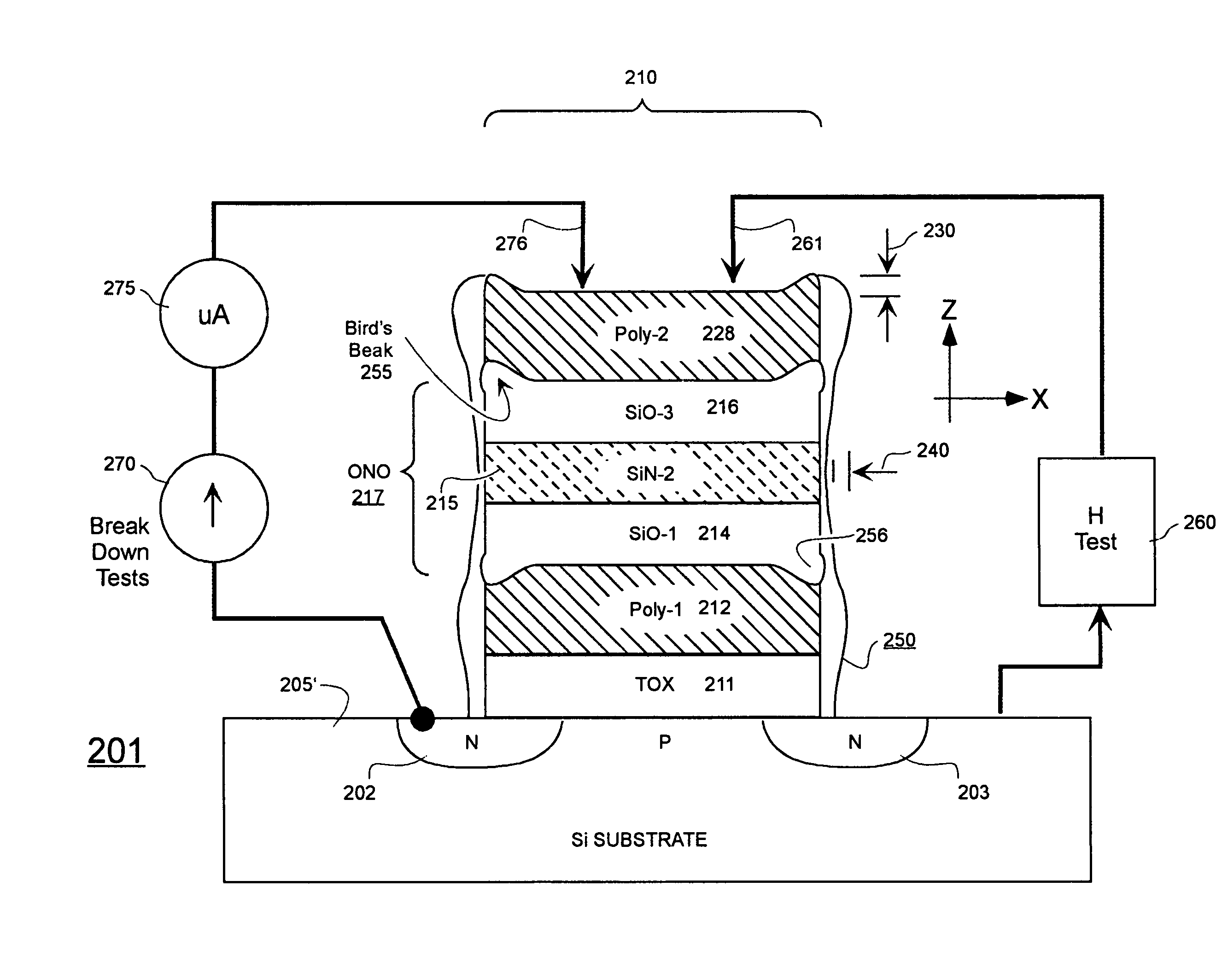
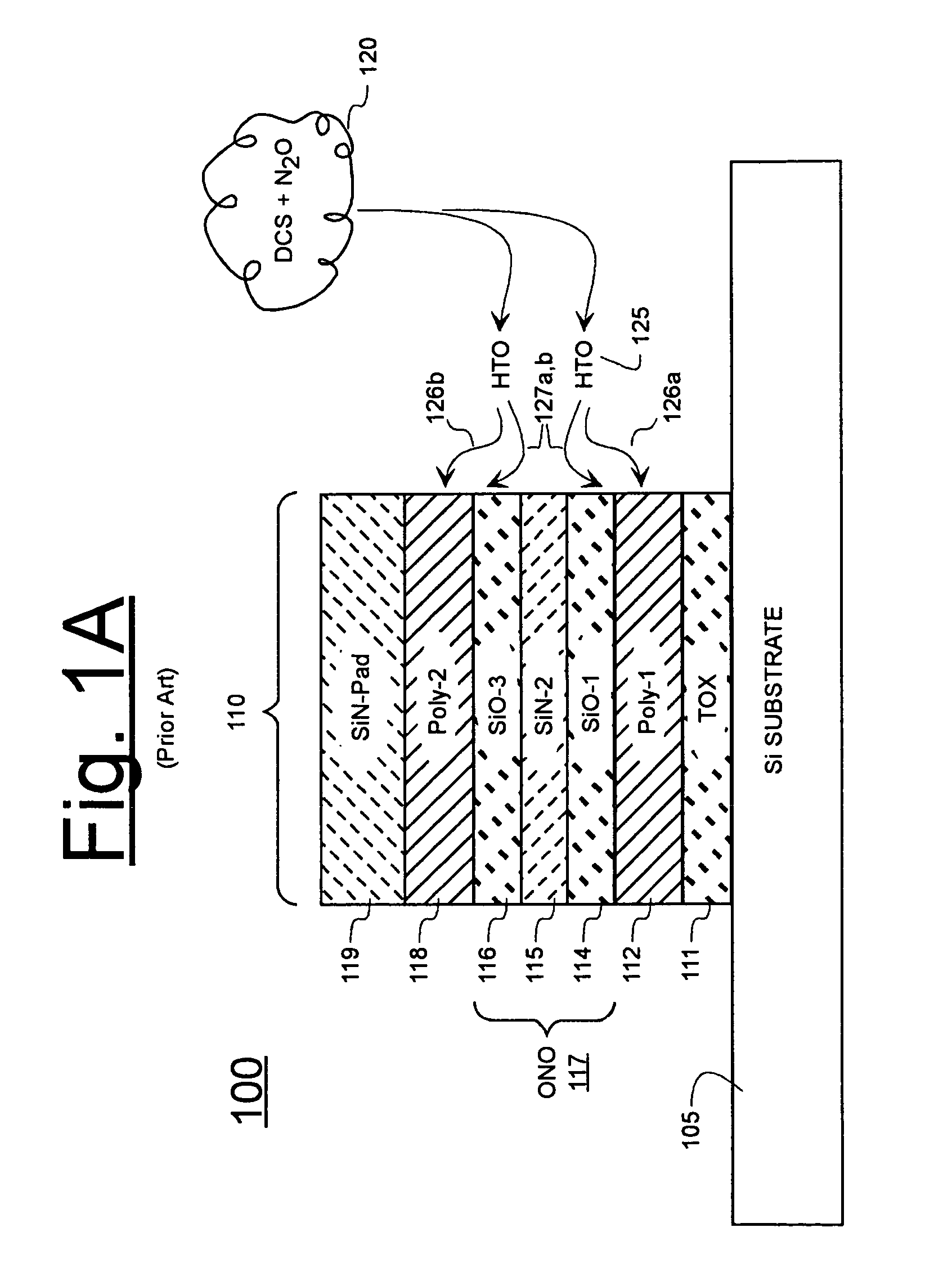
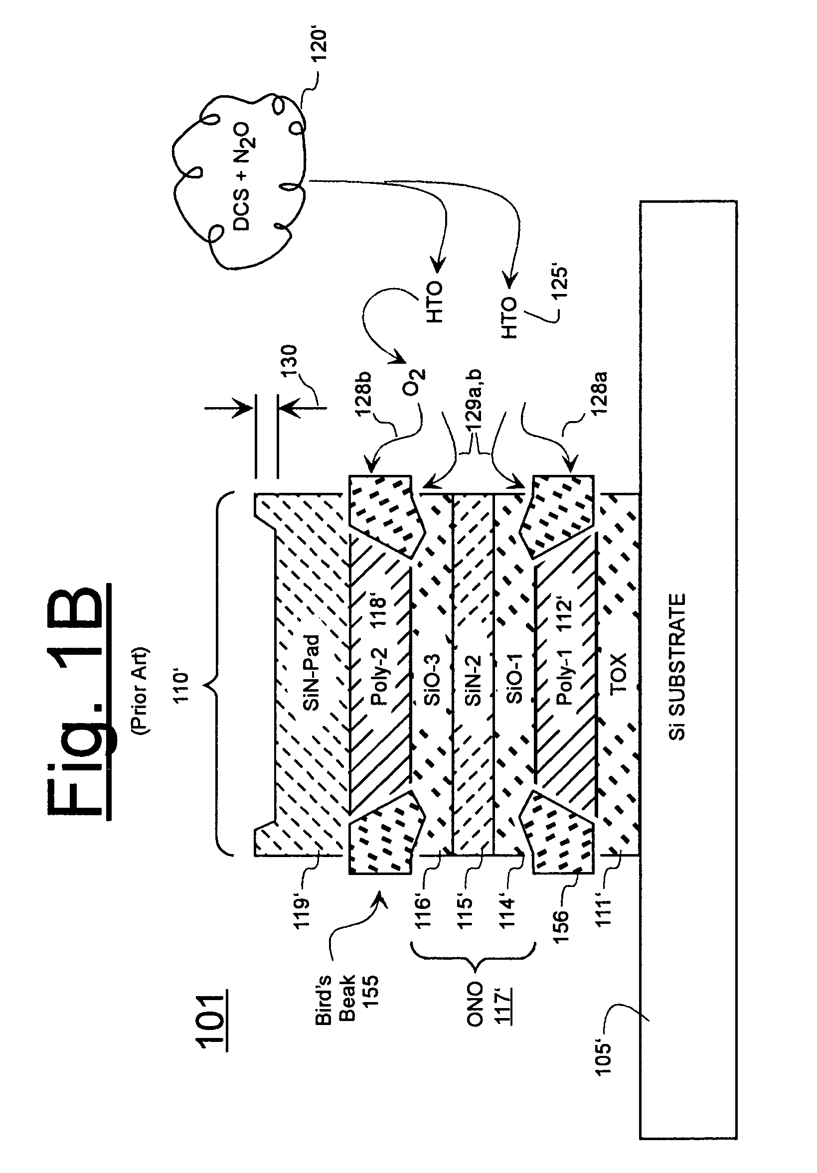
FIG. 1A is a schematic, side cross sectional diagram showing the start of a conventional deposition process 100 wherein oxide sidewall material is to be formed on the sidewalls of a pre-formed and pre-patterned ONO memory cell stack 110 by way of a conventional chemical vapor deposition (CVD) process.

More specifically, a monocrystalline silicon substrate 105 has been provided prior to the start of the sidewall oxidation process. A so-called, tunnel oxide layer (TOX) 111 has been formed on the substrate by thermal growth or otherwise. A first polysilicon layer (Poly-1) 112 has been deposited for later defining the so-called, floating gate (FG) of a corresponding memory cell. On top of the Poly-1 layer 112, a first silicon oxide layer (SiO-1) 114 has been formed to begin definition of the so-called, ONO stack 117. This has been followed by deposition of a silicon nitride layer (SiN-2) 115 and subsequent deposition of a second silicon oxide layer (SiO-3) 116. The triad of the SiO-1 lay...


PUM


Abstract

Conventional fabrication of sidewall oxide around an ONO-type memory cell stack usually produces Bird's Beak because prior to the fabrication, there is an exposed sidewall of the ONO-type memory cell stack that exposes side parts of a plurality of material layers respectively composed of different materials. Certain materials in the stack such as silicon nitrides are more difficult to oxidize than other materials in the stack such polysilicon. As a result oxidation does not proceed uniformly along the multi-layered height of the sidewall. The present disclosure shows how radical-based fabrication of sidewall dielectric can help to reduce the Bird's Beak formation. More specifically, it is indicated that short-lived oxidizing agents (e.g., atomic oxygen) are able to better oxidize difficult to oxidize materials such as silicon nitride and the it is indicated that the short-lived oxidizing agents alternatively or additionally do not diffuse as deeply through already oxidized layers of the sidewall such as silicon oxide layers. As a result, a more uniform sidewall dielectric can be fabricated with more uniform breakdown voltages along it height.

Description

CROSS REFERENCE TO CO-OWNED APPLICATIONSThe following copending U.S. patent applications are owned by the owner of the present application, and their disclosures are incorporated herein by reference:(A) Ser. No. 10 / 442,759 filed May 20, 2003 by Zhong Dong et al. and which is originally entitled, Methods for Improving Quality of High Temperature Oxide (HTO) Formed from Halogen-Containing Precursor and Products Thereof and Apparatus Therefor.FIELD OF DISCLOSUREThe present disclosure of invention relates generally to fabrication of monolithically integrated semiconductor devices.The disclosure relates more specifically to the formation of sidewall insulation for a charge-retaining structure used in non-volatile reprogrammable memory such as the type generically known as an ONO stack.DESCRIPTION OF RELATED ARTSo-called, FLASH memory devices and alike forms of electrically re-programmable and nonvolatile memory devices have become commercially popular due in part to their ability to stor...

Claims


Application Information

Patent Timeline
Patent Type & Authority Patents(United States)
IPC IPC(8): H01L21/336H01L21/28H01L29/423H01L29/51H01L29/788
CPCH01L21/28273H01L29/7881H01L29/513H01L29/42328H01L29/40114
Inventor DONG, ZHONGJANG, CHUCKCHEN, CHING-HWAHUANG, CHUNCHIEHKIM, JIN-HOCHAN, VEI-HANLEUNG, CHUNG WAIHSIAO, CHIA-SHUNKOVALL, GEORGEYANG, STEVEN MING
Owner PROMOS TECH INC
Why Eureka
Try Eureka