Supercharge Your Innovation With Domain-Expert AI Agents!

Method and resulting structure for mosaic of multi-transmission rate optical mask structures

a multi-transmission rate, optical mask technology, applied in the field of integrated circuits, can solve the problems of many limitations, large cost of ic fabrication facilities, and difficulty in small devices, and achieve the effect of high device yield in dies per wafer and convenient us

Active Publication Date: 2011-03-29
SEMICON MFG INT (SHANGHAI) CORP
View PDF4 Cites 0 Cited by
  • Summary
  • Abstract
  • Description
  • Claims
  • Application Information

AI Technical Summary

Benefits of technology

The present invention provides a method and structures for manufacturing semiconductor devices using a multi-transmission rate optical mask. This mask can be used for making different sized patterns with a single light source and mask structure. The invention has a higher device yield in dies per wafer and is compatible with conventional process technology without substantial modifications. The technical effects of the invention include easier use of conventional technology, higher device yields, and compatibility with conventional process technology.

Problems solved by technology

An IC fabrication facility can cost hundreds of millions, or even billions, of dollars.
Making devices smaller is very challenging, as each process used in IC fabrication has a limit.
Although fabless chip companies and foundry services have increased through the years, many limitations still exist.
For example, mask sets used for the manufacture of the custom integrated circuits are often expensive.
That is, they can cost hundreds of thousands of U.S. dollars and take along lead-time to make.
Additionally, there are a limited amount of mask shops that manufacture masks, also leading to difficulty in procuring the mask sets for the custom integrated circuits.

Method used


Image

  • Method and resulting structure for mosaic of multi-transmission rate optical mask structures
  • Method and resulting structure for mosaic of multi-transmission rate optical mask structures
  • Method and resulting structure for mosaic of multi-transmission rate optical mask structures

Examples


examples

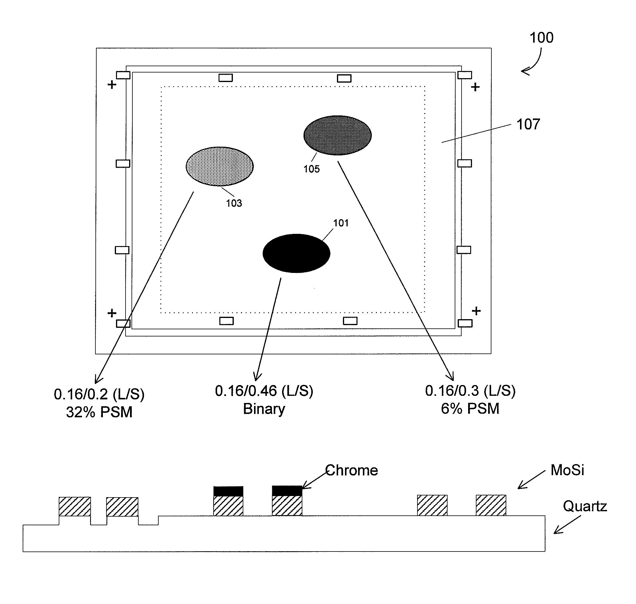
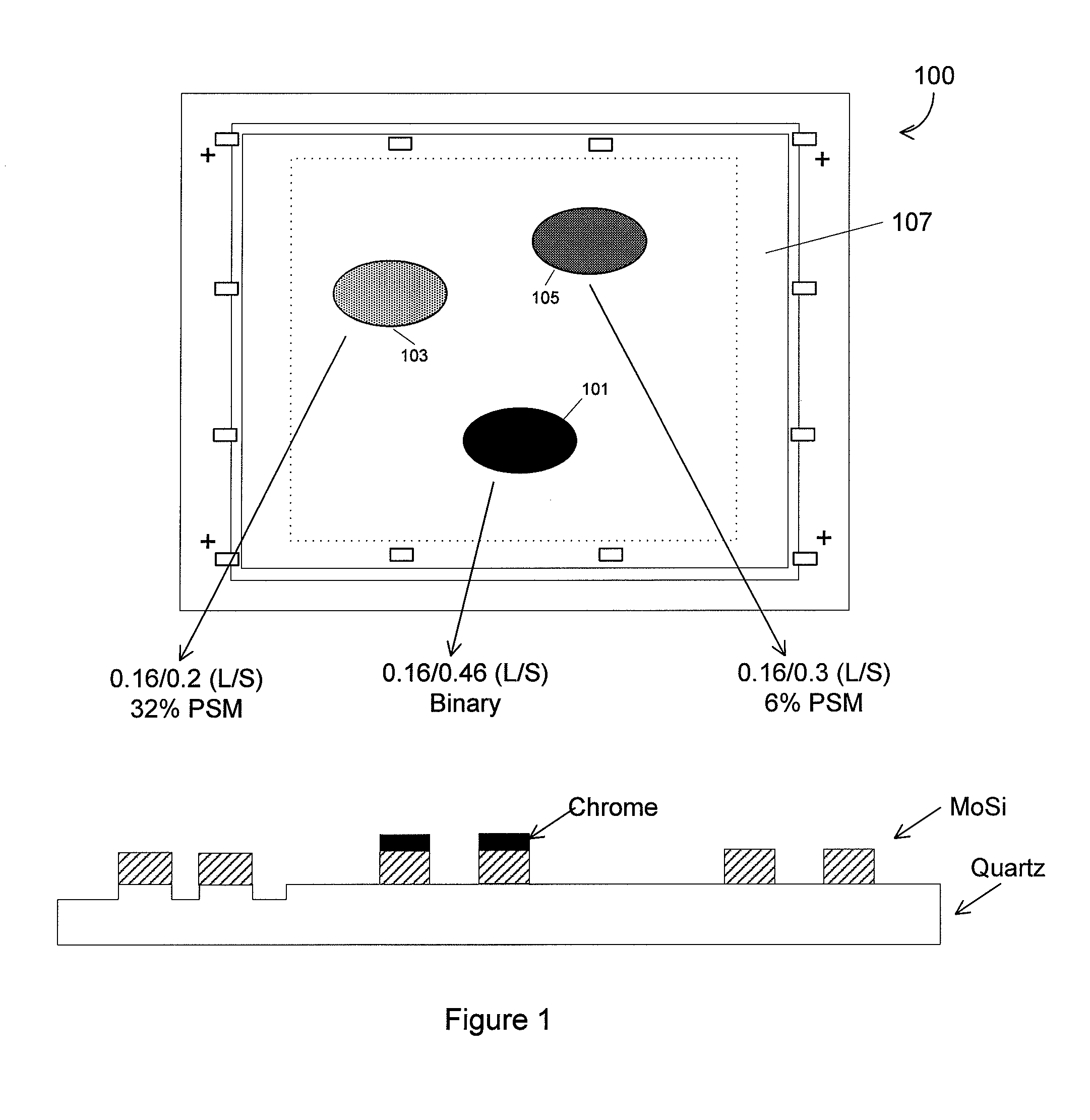
[0024]To prove the operation and method of the present invention, we performed certain experiments to implement aspects of the invention. These experiments are merely examples, which should not unduly limit the scope of the claims herein. One of ordinary skill in the art would recognize other variations, alternatives, and modifications.

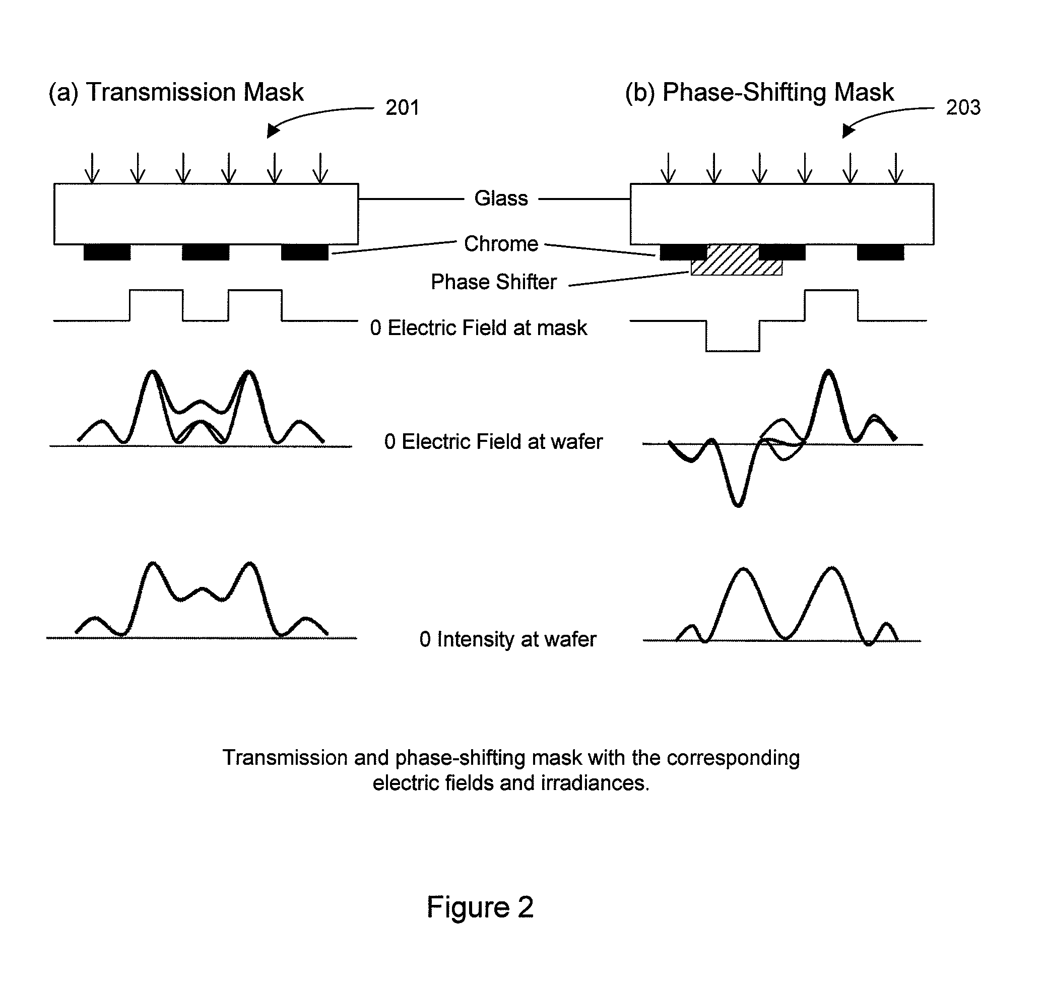
[0025]As background, the attenuated Phase Shift Mask has been widely used for current IC manufacturing companies. The most popular is 6% attenuated phase shift mask (“PSM”). Unfortunately, for a constant transmission rate PSM (like 6%) has intrinsic optical limitation when it comes to multi-pitch layout, which means overlapping DOF (Depth of Focus) for through-pitch designs will be not robust enough for manufacturing. Depth of focus is illustrated by FIG. 5, for example. We have performed certain simulations in these experiments. Such simulations have indicated that, high transmission masks provide benefits over the conventional transmission ones in t...


PUM

PropertyMeasurementUnit
widthaaaaaaaaaa
widthaaaaaaaaaa
widthaaaaaaaaaa

Abstract

A reticle device. The device has a quartz substrate, which has a surface region. A first region comprising a plurality of binary mask patterns is formed on a first portion of the surface region. A second region comprising a plurality of first phase shift mask patterns is formed on a second portion of the surface region. A third region comprising a plurality of second phase shift mask patterns is formed on a third portion of the surface region. Accordingly, the reticle device has at least three different regions corresponding to different optical characteristics.

Description

BACKGROUND OF THE INVENTION[0001]The present invention is directed to integrated circuits and their processing for the manufacture of semiconductor devices. More particularly, the invention provides a method and structures for a multi-transmission rate optical mask structure for manufacture of semiconductor devices. Merely by way of example, the invention has been applied to the manufacture of advanced integrated circuit devices, but it would be recognized that the invention has a much broader range of applicability.[0002]Integrated circuits or “ICs” have evolved from a handful of interconnected devices fabricated on a single chip of silicon to millions of devices. Current ICs provide performance and complexity far beyond what was originally imagined. In order to achieve improvements in complexity and circuit density (i.e., the number of devices capable of being packed onto a given chip area), the size of the smallest device feature, also known as the device “geometry”, has become s...

Claims


Application Information

Patent Timeline
Patent Type & Authority Patents(United States)
IPC IPC(8): G03F1/00
CPCG03F1/32
Inventor HUNG, CHI YUANZHANG, BIN
Owner SEMICON MFG INT (SHANGHAI) CORP
Features
  • R&D
  • Intellectual Property
  • Life Sciences
  • Materials
  • Tech Scout
  • Unparalleled Data Quality
  • Higher Quality Content
  • 60% Fewer Hallucinations
Learn More